
Professional PCB manufacturing and assembly
Building 6, Zone 3, Yuekang Road,Bao'an District, Shenzhen, China
+86-13410863085Mon.-Sat.08:00-20:00

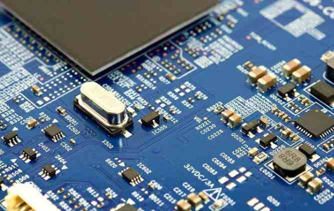
kingford is a professional PCB design company with many years of work experience PCB design team, can provide multi-layer, high density, high speed pcb routing design and PCB design proofing services. Next, we introduce how to control the creepage distance and clearance distance in high voltage PCB design.
When does PCB design security require specific spacing rules?
Not every PCB design has the same strict rules as the spacing required for high voltage PCB designs. In general, if your product's normal operating voltage is at or above 30 VAC or 60 VDC, then you should be very diligent about considering spacing rules in board design. If you have high density boards, especially high voltage boards, you need to be more concerned. High density makes spacing trickier and more important for protection.
Spacing is more important in high voltage designs because the voltage across the board components makes arcing between the two conducting components more likely to occur on your PCB. Any electric arcs that do occur pose a higher risk to both the product and the user. To help reduce risk, PCB design, clearance and creepage distance have two main spacing measurement criteria.
What is PCB design Gap?
Clearance is the shortest distance between two conductors through air. I think the definition is to allow for clearance; How much space was in the air before I hit my head on something. If the gap is too small at any location on the PCB, an overvoltage event may create an arc between adjacent conducting components on the board.
Clearance rules vary with PCB material, voltage and environmental conditions. The environmental impact is significant. Most commonly, humidity changes the breakdown voltage of the air and affects the likelihood of arc discharge. Dust is another standard factor, as particles that gather on the PCB's surface form tracks over time, shortening the distance between conductors.
Arcing can damage your product and users, so spacing on the board is a key design parameter.
What is PCB design creepage distance?
Similar to the gap, the creepage distance measures the distance between conductors on a PCB. However, instead of measuring the distance in the air, it measures the shortest distance along the surface of the insulating material. Board materials and environment also affect creepage distance requirements. The buildup of water or particles on the circuit board can shorten the creepage distance as it was cleared.
When you have a high density design, creepage can be a difficult requirement to meet. Since moving orbit is rarely the first choice, there are other tricks to adding surface distance to your design. By adding slots or vertical isolation barriers between tracks, the creepage distance can be significantly increased without changing the wiring layout on the board.
Consider comparing tracking index (CTI of your material)
After the operating voltage, the most important factor in the clearance and leakage requirements comes from the material properties of the PCB. The electrical insulation of a material is represented by a "comparative tracking index" or CTI value. CTI is the voltage, determined by a standard test, that measures when a material surface fails.

There are zero to five categories, depending on the breakdown value of the material. The mandatory insulation levels of a product are based on these CTI categories. Category 5 is the lowest, with a value less than 100 V. For 600+ V failures, Category 0 has the most powerful and often expensive material options.
PCB insulator materials have different breakdown voltages and corresponding product application safety categories.
What should I do? Know what materials to use and spacing?
Because there are so many variables in PCB design and material selection, the best option to meet safety requirements and standards is to go straight to the source. There are two criteria I refer to most often. The first is IPC-2221, which is the universal standard for PCB design clearance and creepage distance guidance. The second is IEC-60950-1 (2nd Edition). The IEC version is the standard you want to read for any IT product with an AC main power supply or battery power supply, especially if you want to sell these products internationally.
Since the consequences of incorrect spacing are severe death and destruction due to non-compliance with the law, it is well worth taking the time to familiarize yourself with any standards associated with your design. In addition, it prevents undergraduates from self-destructing.
Identifying and merging standards can be time-consuming, so you should use good design software. The best software for PCB design lets you create specific design rules and helps you spot problems early in the process. AltiumDesigner® meets these requirements and more; You can start designing before you choose board insulation!
Shenzhen kngford circuit board design capability
Maximum signal design rate: 10Gbps CML differential signal;
Maximum number of PCB design layers: 40;
Minimum line width: 2.4mil;
Minimum line spacing: 2.4mil;
Minimum BGA PIN spacing: 0.4mm;
Minimum mechanical hole diameter: 6mil;
Minimum laser drilling diameter: 4mil;
Maximum number of pins:; 63000 +
Maximum number of components: 3600;
Maximum number of BGA: 48+.
PCB design service process
1. The customer provides schematic diagram to consult PCB design;
2. Evaluate quotation according to schematic diagram and customer design requirements;
3. The customer confirms the quotation, signs the contract and pays the project deposit;
4. Received advance payment and arranged engineer design;
5. After the design is completed, provide the screenshot of the document to the customer for confirmation;
6. The customer confirmed OK, settled the balance, and provided PCB design materials.
How to select SMT chip inductor?
Mar 15,2023


Just upload Gerber files, BOM files and design files, and the KINGFORD team will provide a complete quotation within 24h.