Have you seen the selective soldering technology of PCB?
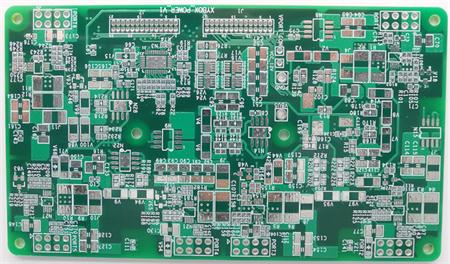
Understand PCB design, PCB layout and PCB manufacturing in PCB industry Have you seen the selective soldering technology of PCB?


Understand PCB design, PCB layout and PCB manufacturing in PCB industry Have you seen the selective soldering technology of PCB?

Understand PCB design, PCB layout and PCB manufacturing in PCB industryUnderstand how to reduce PCB proofing design risk
The circuit board manufacturer and circuit board designer explain the precautions for PTF printing on PET
Understand PCB design, PCB layout and PCB manufacturing in PCB industryCost waste of PCB production and countermeasures
The circuit board manufacturer and circuit board designer explain the limitations of SMT using "Yin Yang" or "Mandarin Duck"
PCB manufacturers and PCB designers explain PCB copper foil thickness, line width and maximum load current
The circuit board manufacturer and circuit board designer explain the solution to the micro short circuit of CAF circuit board
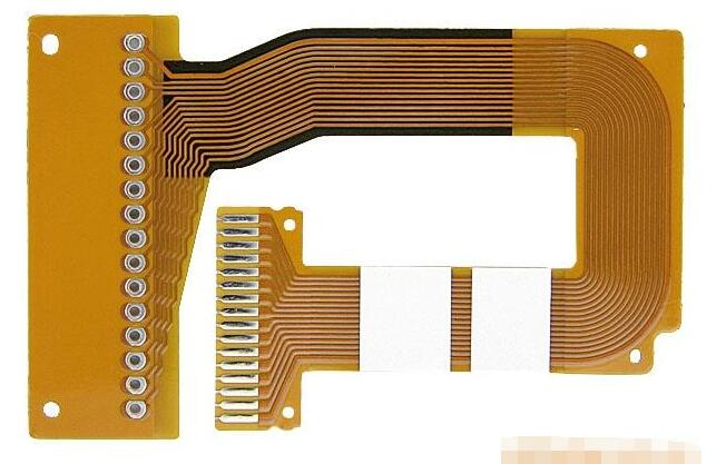
The circuit board manufacturer and circuit board designer will explain the FPC structure - single panel and single copper double fabrication.

This article mainly introduces the interference analysis and countermeasures in high-frequency PCB design

This article mainly introduces the advantages of FPC flexible circuit board and the main application of fast detection of PCB failure
This article mainly introduces the advantages and main applications of FPC flexible circuit board
This article mainly introduces the causes and troubleshooting of PCB nickel electroplating process


