
Professional PCB manufacturing and assembly
Building 6, Zone 3, Yuekang Road,Bao'an District, Shenzhen, China
+86-13410863085Mon.-Sat.08:00-20:00


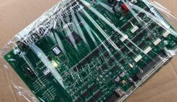
The PCB circuit board is based on the circuit principle diagram to achieve the functions required by the circuit user. The design of PCB mainly refers to the layout design, which requires the layout of internal electronic components, metal wires, through holes and external connections, electromagnetic protection, heat dissipation, crosstalk and other factors. Do you know PCB cleaning technology? Here are some tips to share:
PCB board cleaning technology:
1. Water cleaning technology
Cleaning technology is the development direction of cleaning technology in the future, and it is necessary to set up pure water source and discharge water treatment workshops. It uses water as a cleaning medium, and adds surfactants, auxiliaries, corrosion inhibitors, chelating agents in water to form a series of water-based cleaning agents. Water solvent (flux is water soluble) and non-polar contaminants can be removed.

2. Water cleaning is mainly used organic solvents and deionized water, plus a certain amount of active agents, additives composed of cleaning agents. This kind of cleaning is between solvent cleaning and water cleaning. These cleaning agents are organic solvents, flammable solvents, flash point is relatively high, relatively low toxicity, relatively safe to use, but must be rinsed with water, and then dried. Some cleaning agents add 5% to 20% water and a small amount of surfactants, which both reduces flammability and makes rinsing easier.
3. No-cleaning technology
The use of no-clean flux or no-clean solder paste in the welding process, after welding directly into the next process no longer cleaning, no-clean technology is currently the most used an alternative technology, especially circuit board products are basically using no-wash method to replace ODS. At present, many kinds of no-wash flux have been developed at home and abroad.
4. Solvent cleaning technology
Agent cleaning mainly uses the solubility of the solvent to remove contaminants. Solvent cleaning, because of its fast volatilization, dissolution ability is strong, so the circuit board requirements are simple. According to the selected cleaning agent, it can be divided into combustible cleaning agent and non-combustible cleaning agent.
PCB board copying steps are introduced
PCB board copying steps:
First: Get a PCB circuit board, first record the model, parameters, and position of all the components on the paper, especially the direction of the diode, the transistor, and the direction of the IC notch. It is best to take two pictures of the location of the vital parts with a digital camera.
Second: Remove all the devices, and remove the tin in the PAD hole. Clean the PCB board with alcohol, then put it into the scanner, start the POHTOSHOP, sweep the silk screen with color, and print it out for use.
Third: Lightly polish the TOP LAYER and BOTTOM LAYER with water yarn paper until the copper film shines, put it in the scanner, start PHOTOSHOP, and sweep in the two layers separately with color. Note that the PCB board must be placed horizontally and vertically in the scanner, otherwise the scanned image cannot be used, and the scanner resolution is 600.
Fourth: Adjust the contrast and brightness of the canvas, so that the part with copper film and the part without copper film are in strong contrast, and then turn the subgraph to black and white, check whether the lines are clear, if not, repeat this step. If clear, save the image as black and white BMP format files TOP.BMP and BOT.BMP. Use image processing software to convert the size of the picture at this time to 38.64 times the original physical size, and then use BMP to PCB circuit board software for conversion. Note: BMP image should be stored in black and white format, do not store into other color format, otherwise BMP to PROTEL file software can not convert it.
Fifth: Convert the two BMP files into PROTEL files respectively, and transfer two layers into PROTEL. For example, the positions of PAD and VIA in the two layers basically coincide, indicating that the previous steps are done well. If there is deviation, repeat the third step.
Sixth: will TOP. BMP is converted to TOP. The PCB circuit board should be converted to the SILK layer, that is, the yellow layer, and then you trace the line on the TOP layer, and place the device according to the drawing of the second step. Delete the SILK layer when you are finished.
Seventh: will BOT. BMP is converted to BOT. The PCB circuit board should be converted to the SILK layer, that is, the yellow layer, and then you trace the line in the BOT layer. Delete the SILK layer when you are finished.
Eighth: TOP in PROTEL. PCB and BOT. PCB input, combined into a diagram is OK.
Ninth: Use a laser printer to print the TOP LAYER and BOTTOM LAYER to the transparent film (1:1 ratio), put the film on the PCB board, compare whether it is wrong, if it is correct, you are done.
PCB circuit board copper foil basic knowledge
Jun 19,2023


Just upload Gerber files, BOM files and design files, and the KINGFORD team will provide a complete quotation within 24h.