
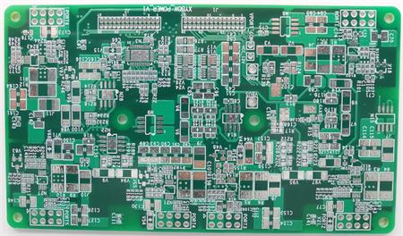
Professional PCB manufacturing and assembly
Building 6, Zone 3, Yuekang Road,Bao'an District, Shenzhen, China
+86-13410863085Mon.-Sat.08:00-20:00

Pit: Ma pit is the result of organic pollution. Large pits usually indicate oil pollution. If the mixing is not good, the bubbles cannot be expelled, which will form pockmarks. Wetting agent can be used to reduce its influence. We usually call small pits pinholes. Pinholes can be generated due to poor pretreatment, metal impurities, too little boric acid content, and too low bath temperature. Bath maintenance and process control are the keys. Anti pinhole agent should be used as process stabilizer to supplement.

Roughness and burr: Roughness indicates that the solution is dirty, which can be corrected by adequate filtration (if the pH is too high, it is easy to form hydroxide precipitation, which should be controlled). If the current density is too high, impurities are brought into the anode mud and impure added water, which will cause roughness and burrs in serious cases.
Low adhesion: If the PCB copper coating is not fully oxidized, the coating will peel off, and the adhesion between copper and nickel is poor. If the current is interrupted, the nickel coating will peel off on its own at the interruption, and it will peel off when the temperature is too low and serious.
Coating brittleness and poor solderability: When PCB coating is bent or worn to some extent, the coating brittleness is usually exposed. This indicates that there is organic matter or heavy metal impurity pollution. Excessive additives, entrained organic matter and electroplating resist are the main sources of organic matter pollution, which must be treated with activated carbon. Insufficient additives and high pH will also affect the brittleness of the coating.
Coating darkening and uneven color: coating darkening and uneven color indicate metal pollution. Since copper plating is generally followed by nickel plating, the copper solution brought in is the main pollution source. It is important to minimize the copper solution on the hanger. In order to remove the metal pollution in the tank, especially the copper removal solution, the corrugated steel cathode should be used. Under the current density of 2~5 A/square inch, 5 amperes per gallon of solution should be empty plated for one hour. Poor pretreatment, poor low coating, too low current density, too low concentration of main salt, and poor contact of electroplating power circuit will affect the coating color.
Plating burn: Possible causes of PCB coating burn: insufficient boric acid, low concentration of metal salt, low working temperature, high current density, high pH or insufficient stirring.
Low deposition rate: low pH value or low current density will cause low deposition rate.
Plating blistering or peeling: poor PCB pre plating treatment, too long intermediate power off time, organic impurity pollution, too high current density, too low temperature, too high or too low pH, and serious impact of impurities will cause blistering or peeling.
Anode passivation: the anode activator is insufficient, the anode area is too small, and the current density is too high. Pit: Ma pit is the result of organic pollution. Large pits usually indicate oil pollution. If the mixing is not good, the bubbles cannot be expelled, which will form pockmarks. Wetting agent can be used to reduce its influence. We usually call small pits pinholes. Pinholes can be generated due to poor pretreatment, metal impurities, too little boric acid content, and too low bath temperature. Bath maintenance and process control are the keys. Anti pinhole agent should be used as process stabilizer to supplement.
PCB
Roughness and burr: Roughness indicates that the solution is dirty, which can be corrected by adequate filtration (if the pH is too high, it is easy to form hydroxide precipitation, which should be controlled). If the current density is too high, impurities are brought into the anode mud and impure added water, which will cause roughness and burrs in serious cases.
Low adhesion: If the PCB copper coating is not fully oxidized, the coating will peel off, and the adhesion between copper and nickel is poor. If the current is interrupted, the nickel coating will peel off on its own at the interruption, and it will peel off when the temperature is too low and serious.
Coating brittleness and poor solderability: When PCB coating is bent or worn to some extent, the coating brittleness is usually exposed. This indicates that there is organic matter or heavy metal impurity pollution. Excessive additives, entrained organic matter and electroplating resist are the main sources of organic matter pollution, which must be treated with activated carbon. Insufficient additives and high pH will also affect the brittleness of the coating.
Coating darkening and uneven color: coating darkening and uneven color indicate metal pollution. Since copper plating is generally followed by nickel plating, the copper solution brought in is the main pollution source. It is important to minimize the copper solution on the hanger. In order to remove the metal pollution in the tank, especially the copper removal solution, the corrugated steel cathode should be used. Under the current density of 2~5 A/square inch, 5 amperes per gallon of solution should be empty plated for one hour. Poor pretreatment, poor low coating, too low current density, too low concentration of main salt, and poor contact of electroplating power circuit will affect the coating color.
Plating burn: Possible causes of PCB coating burn: insufficient boric acid, low concentration of metal salt, low working temperature, high current density, high pH or insufficient stirring.
Low deposition rate: low pH value or low current density will cause low deposition rate.
Plating blistering or peeling: poor PCB pre plating treatment, too long intermediate power off time, organic impurity pollution, too high current density, too low temperature, too high or too low pH, and serious impact of impurities will cause blistering or peeling.
Anode passivation: the anode activator is insufficient, the anode area is too small, and the current density is too high.


Just upload Gerber files, BOM files and design files, and the KINGFORD team will provide a complete quotation within 24h.