
Professional PCB manufacturing and assembly
Building 6, Zone 3, Yuekang Road,Bao'an District, Shenzhen, China
+86-13410863085Mon.-Sat.08:00-20:00

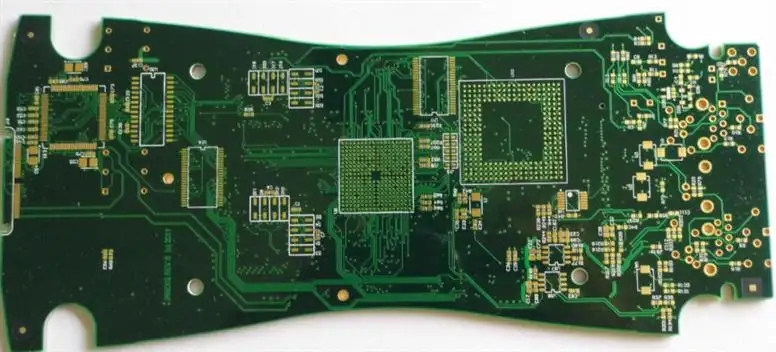
Circuit board factory: Precautions for PTF printing lines on PET
Compared with FPC (Flex Printed Circuit) and PTF (Polymer Thick Film) soft boards, we know that PTF does have many advantages such as low price and short delivery time, but PTF has its previous capacity limitations.
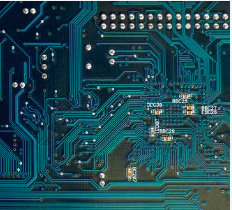
Due to its use of the silk screen process, PFT is unable to produce electronic circuit spacing smaller than FPC. Although PTF claims that the minimum electronic circuit spacing of 5mils (0.12mm) can be achieved, in fact, 10mils (0.25mm) has already reached the limit. In addition, PTF cannot withstand the bending of the dead fold, because the materials of its electronic circuit are silver paste and conductive carbon ink, which are not as good as the copper foil circuit of FPC in ductility and can withstand a limited number of bends.
Foreign matter contamination:
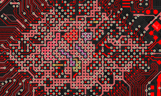
If a non-conductive foreign object sticks to an electronic circuit, its minimum effect is to increase the resistance value of the circuit, because the resistance value is inversely proportional to the area through which electrons pass, and is likely to cause an electrical open circuit; If conductive foreign matters contaminate the lines and between them, it is likely to cause electrical short circuit. This disadvantage is most annoying, because when it is produced in the pcb manufacturing factory, it cannot be screened completely through the testing method. Usually, it will not cause problems until it is installed in the product for a period of time, especially when it is used in the environment of high temperature and humidity. In the future, if you have the opportunity, you can write another article to discuss this topic.
Foreign matters may come from air pollution in the environment, including dust, fiber, paper scraps, etc. Generally speaking, most of them are man-made foreign objects. For example, there are many fibers on clothes, especially sweaters or cotton clothes. Waleng cartons are also a major source of pollution, including hair, paper scraps and fibers, and the human body will always fall off the cuticle. The best prevention and control method is to set up a 100K level clean room with personnel wearing dustproof clothes and strictly controlling various possible pollution sources. Environmental control is really important, especially in the production of products with small spacing lines, because no one can grasp when there will be dirty things on the lines, resulting in irregular quality defects.
Another possible source of foreign matter is ink. When making the ink, some additives of metal components will be added. If these additives are not properly controlled, they may form a hard block. If a larger hard block cannot flow through the screen printed mesh, it will block the screen printed mesh, resulting in printing holes, or even causing the electronic circuit to open; Smaller hard blocks can flow through the mesh, but will form bumps on the electronic circuit. If there are overlapping upper and lower layers of circuits, the bumps are likely to break through the dielectric layer, causing short circuits in the upper and lower circuits. The pollution of printing ink may also come from the bad ambient air during printing ink production or the environment where printing ink is stored. The best way to control ink foreign matters is to filter ink contamination with a filter screen of appropriate size; If the contamination is serious, the coarse filter screen can be used first and then the fine filter screen.
Printing contamination of conductive layer:
When screen printing, the viscosity of conductive ink is very important. When too much thinner is added, the ink will become thinner and easily penetrate into the place where the ink should not have been printed. This disadvantage is called printing contamination. What's worse, the contamination will last until the next printing, or even the next time, until the contaminated ink is exhausted. Serious printing contamination will directly cause short circuit between adjacent conductive lines; Slight printing contamination may also affect the electronic flow between lines. If voltage is used as energy and humidity is used as catalyst, electronic migration is likely to occur between lines. As time goes on, conductivity will occur and short circuit will occur.
The first method to solve the printing contamination of the conductive layer is to select appropriate ink and control the addition of thinner; The second is regular cleaning screen; The third is to strengthen the inspection. It is better to check one piece every time it is done. It would be better if there is an AOI (Auto Optical Inspector).
The circuit board manufacturer and circuit board designer explain the precautions for PTF printing on PET.


Just upload Gerber files, BOM files and design files, and the KINGFORD team will provide a complete quotation within 24h.