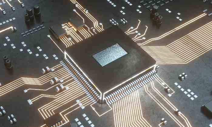
Share PCB routing tips for printed circuit board design
The frequency of the digital circuit is high, the sensitivity of the analog circuit is strong, for the signal line, the high-frequency signal line is as far away from the sensitive analog circuit device as possible, for the ground line, the whole PCB has