
Professional PCB manufacturing and assembly
Building 6, Zone 3, Yuekang Road,Bao'an District, Shenzhen, China
+86-13410863085Mon.-Sat.08:00-20:00

In circuit board design, we are usually very concerned about the quality of the signal, but sometimes we usually limit the research on the signal line, and the power and ground as the ambition of the situation to deal with, although this can make the question simplified, but in high-speed planning, this simplification is now not feasible. Although the direct result of circuit planning comparison is reflected in the signal integrity, we must not neglect the power integrity planning. Because the integrity of the power supply directly affects the signal integrity of the end PCB board. The integrity of the power supply and the integrity of the signal are closely related, and in many cases, the primary cause of signal distortion is the power supply system. For example, the ground rebound noise is too large, the decoupling capacitor planning is not suitable, the loop influence is very severe, the multi-power ground plane cutting is not good, the formation planning is not reasonable, the current is not uniform and so on.

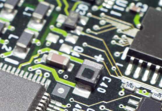
1) Decoupling capacitor
We all know that adding some capacitors between the power supply and the ground can reduce the noise of the system, but in the end, how many capacitors are added to the circuit board, how much the capacity of each capacitor is suitable for what direction each capacitor is placed is very good. These questions are usually not thought about carefully, only by the experience of planners, and sometimes even think that the less the better. In high-speed planning, it is necessary to think about the parasitic parameters of the capacitor, quantitatively calculate the number of decoupling capacitors and the capacity value of each capacitor and the detailed orientation of the placement, to ensure that the impedance of the system is within the control scale, a fundamental principle is that the decoupling capacitors required can not be less, and the remaining capacitors are not required.
2) Ground rebound
When the marginal rate of high-speed devices is less than 0.5ns, the data exchange rate from the negative capacity data bus is particularly fast, and when it occurs in the power layer strong enough to affect the signal, the power instability problem occurs. When the current passing through the ground loop changes, because the inductance of the loop will produce a voltage, when the rising edge is shortened, the current change rate increases, and the ground rebound voltage is added. At this point, the ground plane (ground) is not the desired zero level, and the power supply is not the desired direct current potential. When the gate circuit that switches together is added, the ground bounce becomes more severe. For a 128-bit bus, there can be 50_100 IO lines switching along the same clock edge. At this time, the reaction to the switching of the IO driver's power supply and the inductance of the ground loop must be as low as possible, otherwise, the connection to the same ground stop will present a voltage brush. Ground rebound can be seen everywhere, such as chips, packages, connectors or circuit boards, which can appear to rebound, and then cause questions about the integrity of the power supply.
From the point of view of skill development, the rising edge of the device will only be reduced, and the width of the bus will only be added. The only way to stick to the acceptable rebound is to cut the power supply and ground spread the inductance. For the chip, it means moving to an array of chips, placing as much power and ground as possible, and the connection to the package can be as short as possible to reduce inductance. Regarding, packaging, means moving layer packaging, so that the distance between the ground plane of the power supply is closer, as used in the BGA package top. For connectors, this means using more ground pins or planning the connector from scratch so that it has an internal power supply and ground plane, such as ribbon cords according to the connector. In terms of circuit boards, it means making adjacent power sources and ground planes as close as possible. Because the inductance is proportional to the length, the connection between the power supply and the ground can be as short as possible to reduce the ground noise.
Power integrity planning is a very complex work, but how to control the impedance between the power system (power supply and ground plane) in recent years is the key to planning. In theory, the lower the impedance between the power supply system, the better, the lower the impedance, the smaller the noise fluctuation, the smaller the voltage loss. In practical planning, we can determine the policy impedance we expect to reach by rules of the maximum voltage and power supply change scale, and then adjust the relevant elements in the circuit to make the impedance of each part of the power system (related to frequency) policy impedance to the emergency.


Just upload Gerber files, BOM files and design files, and the KINGFORD team will provide a complete quotation within 24h.