
Professional PCB manufacturing and assembly
Building 6, Zone 3, Yuekang Road,Bao'an District, Shenzhen, China
+86-13410863085Mon.-Sat.08:00-20:00

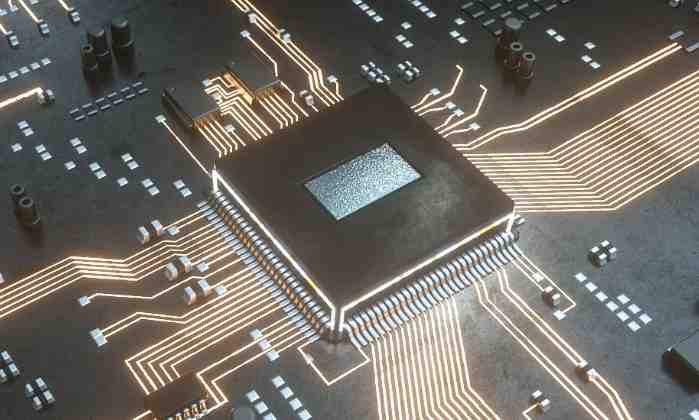
Right Angle wiring is generally required to avoid the situation in PCB wiring, and it has almost become one of the standards to measure the quality of wiring, so how much impact will right Angle wiring have on signal transmission? In principle, right-angle wiring will cause the line width of the transmission line to change, resulting in impedance discontinuity. In fact, not only right Angle wiring, ton Angle, acute Angle wiring may cause impedance changes. The impact of right-angle wiring on the signal is mainly reflected in three aspects: first, the corner can be equivalent to the capacitive load on the transmission line, slowing down the rise time; Second, impedance discontinuity will cause signal reflection; The third is the EMI generated by the right Angle tip.

The parasitic capacitance caused by the right Angle of the transmission line can be calculated by the following empirical formula: C=61W(Er)1/2/Z0 In the above formula, C is the equivalent capacitance of the corner (unit: pF), W is the width of the line (unit: inch), εr is the dielectric constant of the medium, and Z0 is the characteristic impedance of the transmission line. For example, for a 4Mils 50 ohm transmission line (εr is 4.3), the capacitance of a right Angle is approximately 0.0101pF, and the resulting change in rise time can be estimated: T10-90%=2.2*C*Z0/2 =2.2* 0.0101*50/2 = 0.556ps It can be seen from the calculation that the capacitance effect brought by right-angle wiring is extremely small.
As the line width of the right-angle line increases, the impedance there will decrease, so a certain signal reflection phenomenon will be generated, we can calculate the equivalent impedance after the line width increase according to the impedance calculation formula mentioned in the transmission line chapter, and then calculate the reflection coefficient according to the empirical formula: ρ=(ZS-Z0)/(Zs+Z0), generally the impedance change caused by right-angle wiring is between 7% and 20%, so the reflection coefficient is maximum about 0.1. Moreover, as can be seen from the figure below, the transmission line impedance changes to the minimum within the W/2 line length time, and then returns to the normal impedance after the W/2 time, the entire impedance change time is very short, often within 10ps, so fast and small changes for the general signal transmission is almost negligible.
Many people have such an understanding of right-angle wiring, that the tip is easy to emit or receive electromagnetic waves, resulting in EMI, which has become one of the reasons why many people think that right-angle wiring is not possible. However, many practical tests have shown that right-angled lines do not produce significantly more EMI than straight lines. Perhaps the current performance of the instrument, the test level limits the accuracy of the test, but at least illustrates a problem, the radiation of the right Angle line has been less than the measurement error of the instrument itself.
All in all, the right Angle line is not so terrible as imagined. At least in applications below GHz, any effects such as capacitance, reflection, EMI, etc. generated by it are almost not reflected in TDR tests, and the focus of high-speed PCB design engineers should still be placed on layout, power/ground design, routing design, through holes and other aspects. Of course, although the impact of right-angle wiring is not very serious, but it does not mean that we can walk right angles in the future, attention to detail is the basic quality necessary for every good engineer, and, with the rapid development of digital circuits, PCB engineers processing signal frequency will continue to improve, to more than 10GHz RF design field, These little right angles can become the focus of high-speed problems.
4 Chemical tin
Chemical tin is the most copper-tin displacement reaction.
Advantages of chemical tin:
Suitable for horizontal line production.
Suitable for fine line processing, suitable for lead-free welding, especially suitable for crimping technology.
Very good flatness, suitable for SMT.
Chemical tin weaknesses:
Good storage conditions are required, preferably not more than 6 months, to control tin whisker growth.
Not suitable for contact switch design
In the production process, the welding resistance film process is relatively high, otherwise it will cause the welding resistance film to fall off.
For multiple welding, N2 gas protection is best.
Electrical measurement is also a problem.
5 Chemical Nickel Gold (ENIG)
Nickel gold is a relatively large application of a surface treatment process, remember: nickel layer is nickel phosphorus alloy layer, according to PCB proofing phosphorus content is divided into high phosphorus nickel and phosphorus nickel, the application is not the same, here does not introduce the difference.
Advantages of nickel gold:
Suitable for lead-free welding.
Very flat surface, suitable for SMT.
Holes can also be coated with nickel gold.
Long storage time, storage conditions are not harsh.
Suitable for electrical testing.
Suitable for switch contact design.
Suitable for aluminum wire binding, suitable for thick plate, strong resistance to environmental attack.


Just upload Gerber files, BOM files and design files, and the KINGFORD team will provide a complete quotation within 24h.