
Professional PCB manufacturing and assembly
Building 6, Zone 3, Yuekang Road,Bao'an District, Shenzhen, China
+86-13410863085Mon.-Sat.08:00-20:00

Radio frequency (RF) board design Although there are many uncertainties in theory, there are many rules that can be followed in RF board design. However, in the actual design, the really practical technique is how to compromise these rules when they cannot be implemented due to various limitations, and this article will focus on the various issues related to RF board partition design.
1. Types of micro-pores
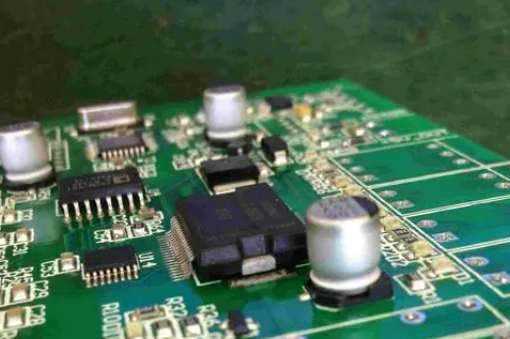
Circuits of different nature on the board must be separated but connected in the best case without electromagnetic interference, which requires the use of microvia. Usually the diameter of the microholes is 0.05mm to 0.20mm, and these holes are generally divided into three categories, namely blind via, bury via and through via. Blind holes are located on the top and bottom surfaces of the printed circuit board and have a certain depth for the connection of the surface circuit and the inner circuit below, and the depth of the holes usually does not exceed a certain ratio (aperture). The buried hole refers to the connection hole located in the inner layer of the printed circuit board, which does not extend to the surface of the board. The above two types of holes are located in the inner layer of the board, which is completed by the through hole forming process before lamination, and several inner layers may be overlapped during the formation of the through hole. The third type, called through-holes, runs through the entire circuit board and can be used for internal interconnection or as adhesive positioning holes for components.

2. Use partitioning techniques
When designing RF circuit boards, high power RF amplifier (HPA) and low noise amplifier (LNA) should be isolated as far as possible, simply put, that is, to keep the high power RF transmitting circuit away from the low noise receiving circuit. This can be done easily if there is a lot of space on the PCB board. But usually when there are many components, the PCB space will become small, so it is difficult to achieve. They can be placed on both sides of the PCB board, or have them work alternately, rather than simultaneously. High power circuits may also sometimes include RF buffers (buffers) and voltage-controlled oscillators (VCO).
Design partitioning can be divided into physical partitioning and Electrical partitioning. Physical partition mainly involves the layout, orientation and shielding of components. Electrical partitions can continue to be divided into power distribution, RF wiring, sensitive circuits and signals, and ground.
3. Physical partition
Component layout is the key to achieving a good RF design, and the most effective technique is to first fix the component on the RF path and adjust its orientation to minimize the length of the RF path. And keep the RF input away from the RF output, and as far away as possible from high power circuits and low noise circuits.
The most efficient way to stack the board is to arrange the main ground in the second layer below the surface layer and walk the RF line on the surface layer as much as possible. Minimizing the through-hole size on the RF path not only reduces the path inductance, but also reduces the virtual solder joints on the main ground and reduces the chance of RF energy leaking into other areas within the laminate.
In physical space, linear circuits like multistage amplifiers are usually sufficient to isolate multiple RF regions from each other, but duplexers, mixers, and IF amplifiers always have multiple RF/IF signals interfering with each other, so care must be taken to minimize this effect. RF and IF lines should be crossed as far as possible, and a ground area should be separated between them as far as possible. The correct RF path is very important for the performance of the entire PCB board, which is why component layout usually takes the majority of the time in mobile phone PCB board design.
On a mobile phone PCB board, it is usually possible to place the low-noise amplifier circuit on one side of the PCB board, and the high-power amplifier on the other side, and finally connect them to one end of the RF antenna and the other end of the baseband processor on the same side by means of a diplexer. This requires some tricks to ensure that RF energy is not transferred from one side of the board to the other by passing through holes, a common technique is to use blind holes on both sides. The adverse effects of passing holes can be minimized by arranging blind holes in areas where both sides of the PCB are not subject to RF interference.
4. Metal shield
Sometimes, it is not possible to retain sufficient separation between multiple circuit blocks, in which case it is necessary to consider using metal shields to shield RF energy in the RF region, but metal shields also have side effects, such as high manufacturing and assembly costs.
The metal shield with irregular shape is difficult to ensure high precision in manufacturing, and the rectangular or square metal shield restricts the layout of components. Metal shield is not conducive to component replacement and fault displacement; Because the metal shield must be welded to the ground surface and must be kept at an appropriate distance from the components, it takes up valuable PCB board space.


Just upload Gerber files, BOM files and design files, and the KINGFORD team will provide a complete quotation within 24h.