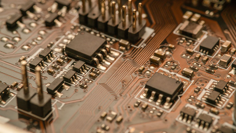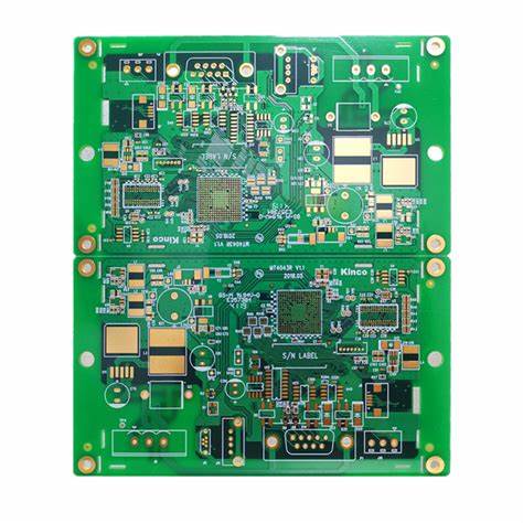
Small batch PCBA assembly
Small batch PCBA assemblyThis is the process involved in PCBA production and assembly by reducing costs while ensuring high quality is maintained. Here, the processes employ various techniques to maintain quality and keep costs down.Techniques used to sec