
Professional PCB manufacturing and assembly
Building 6, Zone 3, Yuekang Road,Bao'an District, Shenzhen, China
+86-13410863085Mon.-Sat.08:00-20:00

PCB manufacturing principle process
The manufacturing process of PCB is relatively complicated, and there are many process requirements. In fact, there are many specific manufacturing processes on the Internet. Let’s talk about the principle of PCB. PCBs are often like layer cakes or lasagnas. If not delicious, but carefully placed alternating layers of different ingredients. They are laminated together using heat and adhesives to form a single unit.
Let's start in the middle and work on that.
The base material or substrate is usually fiberglass. Historically, the most common designation for this fiberglass is "FR4". The fiberglass is stacked on top of each other and secured with resin, making a unit strong enough to hold the boards. There are also flexible PCBs built on flexible high-temperature plastics.
Cheaper PCBs should be made with other materials. Epoxy or phenolic resins lack the durability of FR4, but are much less expensive. These types of substrates can also be found in low-end consumer electronics.
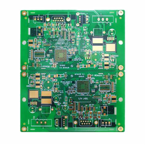
PCBs can be single-sided (one copper layer), double-sided (two copper layers on either side of a substrate layer), or multi-layered (outer and inner copper layers, alternating with substrate layers).
Layer Lasagna or PCB
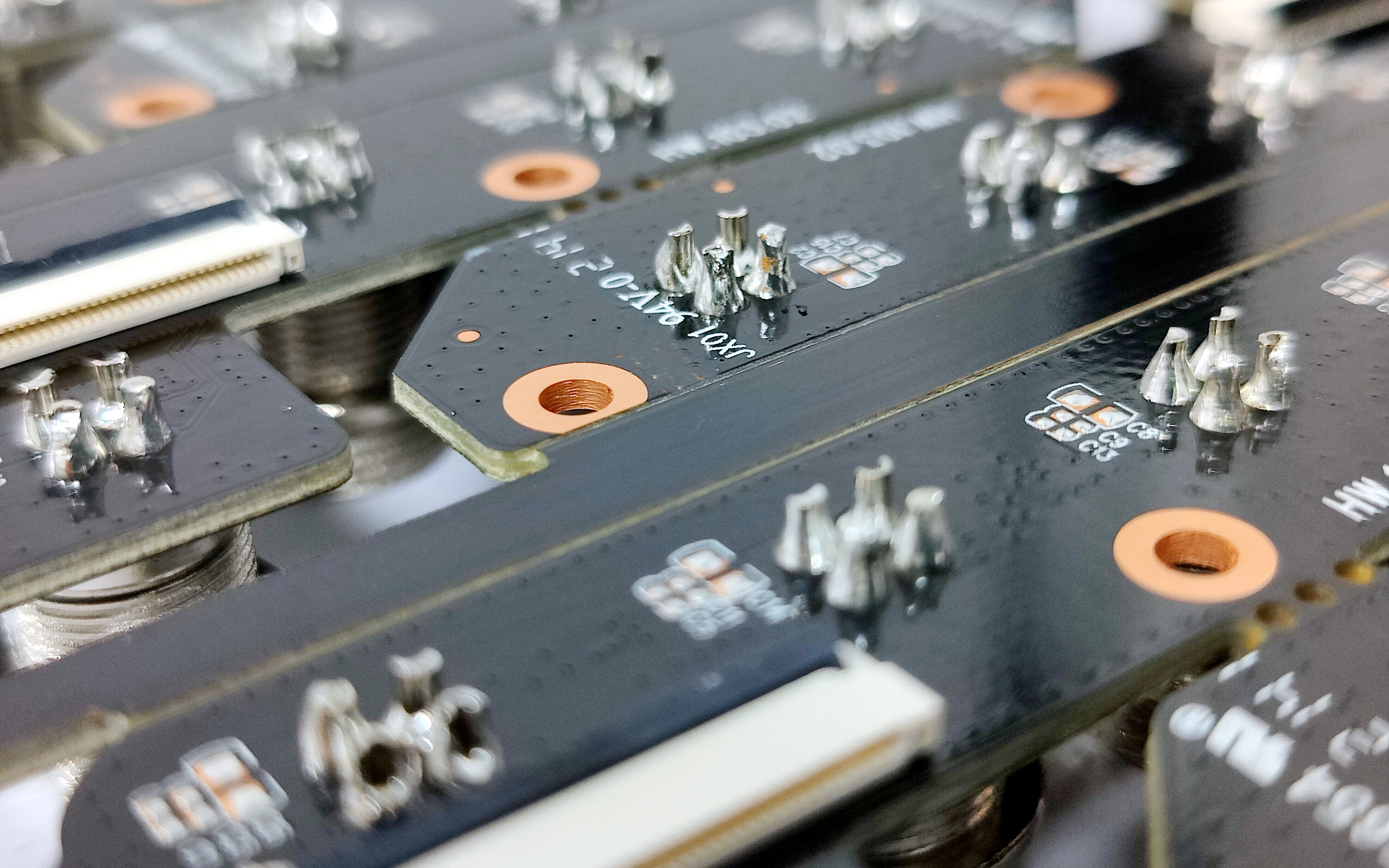
The next layer is thin copper foil. It is laminated to the circuit board with heat and adhesives. Typically, on a double-sided PCB, copper is applied to both sides of the substrate. In less expensive electronics, the PCB may only have copper on one side. When we say double-sided or double-layer board, we mean the number of copper layers in the lasagna.
This lasagna can be made with as few as 1 layer or as many as 16 or more layers.
The layer on top of the copper foil is called the solder mask. This layer gives the typical green color to the PCB. Apply it to the copper layer to insulate the copper traces. It eliminates the possibility of accidental contact with other metals, solder or conductive bits. This layer helps the user solder to precise locations and prevents solder skipping.
Apply a layer of white silkscreen on top of the solder mask. This silkscreen adds letters, numbers and symbols to the PCB. This allows for easier assembly and instructs humans to better understand the board. We often use silkscreen labels to indicate the function of each pin or LED.
A printed circuit board
Now back to our analogy:
On the top of the PCB, you can notice a series of lines running all over the place, connecting various components. Aren't our roads the same, with cities all over the place connecting all places? But here, instead of cars moving around, electrons are flying on copper roads, rushing to power one component after another! These copper tracks are called traces in our PCB city.
A city is where all major engineering takes place. We have offices, local businesses and more on every corner. This center of human activity is like those square black shapes found on PCBs called integrated circuits (ICs). These ICs are where all the hard work in the Double-Sided PCB Assembly place to do the quick calculations.
Suburbs are typical places for homes, parks and schools. From an airplane, you'll notice that suburban rows of houses often look like the little resistors you'd find on a PCB. These resistors significantly control charge flow through resistance.
No city is exempt from construction! Whether building a new skyscraper or a new apartment complex, you'll find new foundations everywhere. These bases are like empty pads without components that you find on PCBs. While they may be empty right now, a component will be soldered to them soon.
Even our PCB cities have their own street names and addresses.
< This form of addressing, called silkscreening, helps the person who assembles or fixes a PCB know exactly where and where a part is.
All the company water we use comes from local storage tanks, who find themselves traveling through pipes to different places. This system is like the holes you would find on a PCB, called vias. These help to get power from one side of the PCB to the other, much like our water goes from our local storage tank to our bathroom, it's a highway.
Power plants in cities keep their lights on. Can you imagine a city without them? Hope it's not zombie infested! Like power plants in cities, we put so-called capacitors on PCBs that store electricity. They hold the charge and release it when it needs to generate electricity.
Streetlights and signs help maintain order in a world full of crazy drivers. They control the flow of traffic on our labyrinthine streets and highways. On PCBs, diodes and their cousins LEDs are those signs and street lights. Diodes control the current flow on the PCB. It allows it to go in only one direction.
Surface assembly method of PCBA processing
Jun 02,2023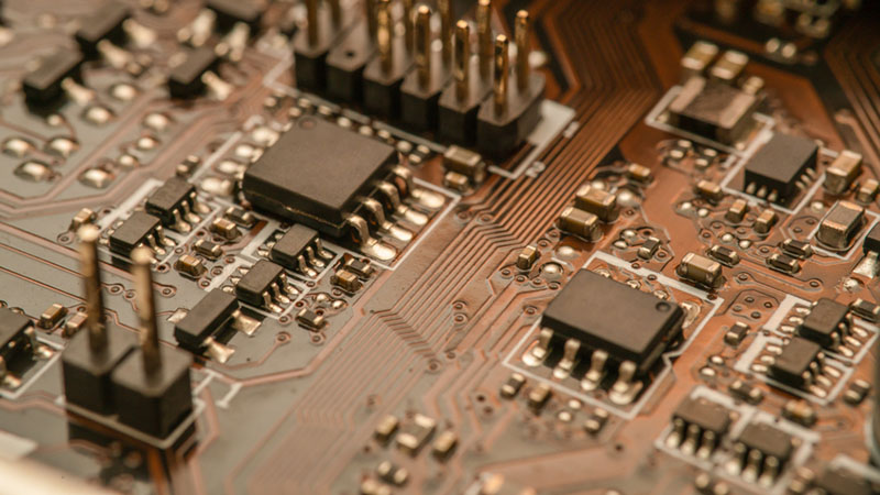


Just upload Gerber files, BOM files and design files, and the KINGFORD team will provide a complete quotation within 24h.