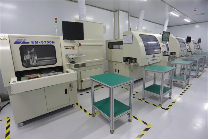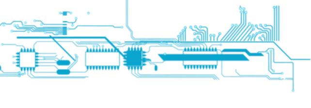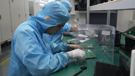
PCB assembly factory introduces DIP plug-in process
The DIP plug-in process is a part of the PCBA process after the SMT patch process. The DIP plug-in process can be roughly divided into plug-in, wave soldering, foot cutting, inspection, testing and other processes.