
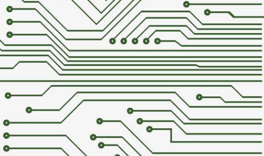
Professional PCB manufacturing and assembly
Building 6, Zone 3, Yuekang Road,Bao'an District, Shenzhen, China
+86-13410863085Mon.-Sat.08:00-20:00

Electromagnetic Compatibility (EMC) refers to the ability of electronic equipment to work harmonically and effectively in various electromagnetic environments. The purpose of EMC design is to enable electronic equipment not only to suppress all kinds of external interference, so that electronic equipment can work properly in a specific electromagnetic environment, but also to reduce the electromagnetic interference of electronic equipment itself to other electronic equipment. Electromagnetic compatibility in the design of printed circuit board (PCB) involves many factors, the following mainly from three parts to be elaborated, the specific selection to integrate various factors.

A printed circuit board overall layout and device layout
1. The success of a product, one is to pay attention to the internal quality, two is to take into account the overall beauty, both are more perfect to consider the product is successful; On a PCB board, the layout of components is required to be balanced, dense and orderly, not top-heavy or heavy, and the hole should be as little as possible; The best shape for a circuit board is a rectangle. Length to width ratio 3:2 or 4:3; The noise of 4-layer board is 20dB lower than that of double panel. The noise of 6-layer board is 10dB lower than that of 4-layer board. When economic conditions permit, use as many layers as possible.
2 circuit board is generally divided into analog circuit area (afraid of interference), digital circuit area (afraid of interference, and interference), power driving area (interference source), so the step board should be reasonably divided into three areas.
3. Devices are generally selected with low power consumption and good stability, and high-speed devices are used as little as possible.
4 line pay attention to: conditions do wide line never do fine; High pressure and high frequency line should be smooth, no sharp chamfering, turning shall not use right angles. Ground should be as wide as possible, the best use of large areas of copper, this docking site problem has considerable improvement.
5. The external clock is a high frequency noise source, which can cause interference to the application system, but also may cause interference to the outside world, so that the electromagnetic compatibility test can not reach the standard. It is one of the principles to reduce the noise in the application system which requires high reliability. Take 8051 MCU as an example, the shortest instruction cycle 1? s time, the external clock is 12MHz, and the same speed Motorola single-chip system clock only 4MHz, more suitable for industrial control system. In recent years, some manufacturers of 8051 compatible single chip microcomputer also adopted some new technology, without sacrificing the premise of computing speed to reduce the external clock demand to 1/3 of the original. And Motorola MCU in the newly launched 68HC08 series and its 16/32 bit MCU generally uses the internal phase-locked loop technology, the external clock frequency down to 32KHz, and the internal bus speed is increased to 8MHz or higher.
6. Wiring should have a reasonable direction: such as input/output, AC/DC, strong/weak signal, high/low frequency, high/low pressure, etc... Their direction should be linear (or separate) and not blend into each other. The aim is to prevent mutual interference. The best direction is in a straight line, but generally not easy to achieve, the most unfavorable direction is a ring. For DC, small signal, low voltage PCB design requirements can be lower. So "reasonable" is relative. The direction of cable routing between the upper and lower layers is basically vertical. The whole board does not want to be uniform, can not be crowded together.
7. In terms of device layout, like other logic circuits, the related devices should be placed as close as possible, so that better anti-noise effect can be obtained. The clock input terminals of the clock generator, crystal oscillator and CPU are easy to generate noise. They should be close to each other, especially do not walk the signal line under the crystal oscillator. It is very important that noisy devices, small current circuits, large current circuits, etc. should be kept away from logic circuits as far as possible. If possible, circuit boards should be made separately.
Two ground technology SkE safety and electromagnetic compatibility network
1. There are many similarities and differences between analog circuits and digital circuits in the design and wiring of component layout diagrams. In the analog circuit, due to the existence of amplifier, the minimal noise voltage generated by wiring will cause serious distortion of the output signal. In the digital circuit, TTL noise tolerance is 0.4V ~ 0.6V, CMOS noise tolerance is 0.3 ~ 0.45 times of Vcc, so the digital circuit has strong anti-interference ability. The reasonable choice of good power supply and ground bus mode is an important guarantee for the reliable operation of the instrument. Quite a lot of interference sources are generated through the power supply and ground bus, among which the ground wire causes the most noise interference.
2. Digital ground and analog ground separate (or a point of ground), ground wire widened, to determine the line width according to the current, generally speaking, the thicker the better (100mil line through about 1 to 2A current). The ground cable > Power cable > Signal cable is a reasonable choice of cable width.
3. The power cable and ground cable should be as close as possible. The power supply on the whole printing board should be distributed in a well shape with the ground, so that the current of the distribution line can be balanced.


Just upload Gerber files, BOM files and design files, and the KINGFORD team will provide a complete quotation within 24h.