
Professional PCB manufacturing and assembly
Building 6, Zone 3, Yuekang Road,Bao'an District, Shenzhen, China
+86-13410863085Mon.-Sat.08:00-20:00

Increase the amount of solder paste to improve BGA welding defects?
How to improve the BGA welding quality has always been one of the quality improvement goals pursued by SMT engineers. Especially for BGA parts with fine pitch, we generally call BGA with a pitch of less than 0.8mm as fine pitch (sometimes there are small differences in definitions).
The reason why BGA is difficult to weld is that its welding points are all concentrated below its body. After welding, it is difficult to check the quality of BGA by visual inspection or AOI (Auto Optical Inspector) image detection instrument. Sometimes it is difficult to judge whether there is empty welding or false welding even using X-Ray. (Some X-Ray or 5DX that can rotate the angle have the opportunity to check the empty welding problem of BGA, but this kind of X-Ray inspection machine is expensive, and it seems that it has not reached the economic scale of mass production with line inspection.
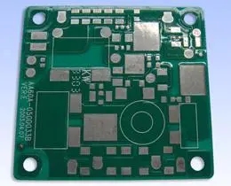
Finished PCB module
Experience tells us that the main quality problems after BGA welding almost all focus on HIP (Head In Pillow, Pillow Effect, Double Ball Effect). This is because PCB and BGA body are prone to deformation when PCB flows through reflow's reflow high temperature area. When solder paste and BGA solder ball are melted into liquid, they are separated from each other and do not contact each other. After the PCB temperature starts to drop and is lower than the melting point of solder, the deformation of PCB and BGA body also gradually decreases. However, solder paste and solder ball have been condensed back to solid state, resulting in a false soldering phenomenon of double ball overlap, which is known as HIP.
While more than 90% of the HIPs appear in the outermost row of solder balls or four corners of the BGA. This is because the BGA package has the longest diagonal distance, and the relative deformation is the most serious. The second most serious deformation is in the outermost row of solder balls of the BGA.
According to the above experience and the experiments conducted by many SMT predecessors, increasing the amount of BGA solder can effectively reduce this kind of HIP problem caused by the deformation of the plate due to temperature. However, be careful that too much solder paste will cause welding short circuit.
Therefore, the method selected below is to increase the amount of BGA solder paste locally instead of increasing the amount of tin for all solder ball pads.
To change the amount of solder paste in BGA, you can start with the steel plate (Stencil). The basic principle is to make the print amount of solder paste in the outermost row or four corners of the BGA more than the amount of solder paste in other solder balls, but not too much, so that when the PCB and the BGA body are deformed, enough solder paste can still be kept in contact with the solder balls under the BGA.
When BGA solder ball is greater than 0.4mm:
Increase the printing amount of solder ball solder paste on the four sides of the BGA periphery, square the steel plate and form an inscribed circle with the original solder ball round pad, and maintain the original amount of other solder ball pads.
When BGA solder ball is less than 0.4mm:
The solder ball paste printing on the four sides of the BGA periphery remains unchanged, but the solder ball on the other inner sides reduces the amount of solder paste. The steel plate is cut into a square to form an outer circle with the original solder ball round pad.
In this way, no matter the size of BGA, the amount of solder paste in the outermost ring of the solder ball will be about 16.7% more than that in the inner ring, to ensure that there is enough solder paste to keep contact with the solder ball under the BGA when PCB and BGA body pass through high temperature deformation.
The following picture shows that the size of the BGA solder ball is less than 0.4mm. The X-Ray is obtained by reducing the amount of solder paste surrounding the ball in the BGA. If you pay a little attention, you can find that the amount of tin on the outermost ring (the diameter of the circle) is a little more than the amount of tin on the other inner ring solder balls. That is, the diameter of the black circle of the outer circle is a little larger than that of the inner circle.


Just upload Gerber files, BOM files and design files, and the KINGFORD team will provide a complete quotation within 24h.