
Professional PCB manufacturing and assembly
Building 6, Zone 3, Yuekang Road,Bao'an District, Shenzhen, China
+86-13410863085Mon.-Sat.08:00-20:00

What are the advantages of SMT components? I will explain them to you
Compared with plug-in components, SMT components have many advantages. Small size, low height, automatic production, good high-frequency characteristics, low cost. SMT components are surface mounted, avoiding the wiring in the inner layer of PCB, and are widely used in some high-end products. SMT components are relatively short, providing competitiveness for many customers seeking thin products. In the production, the placement machine is used for automatic placement, which greatly improves the production efficiency. Its pin less or short pin design improves the high frequency characteristics and has good stability. In addition, low cost is also the eternal pursuit of manufacturers.
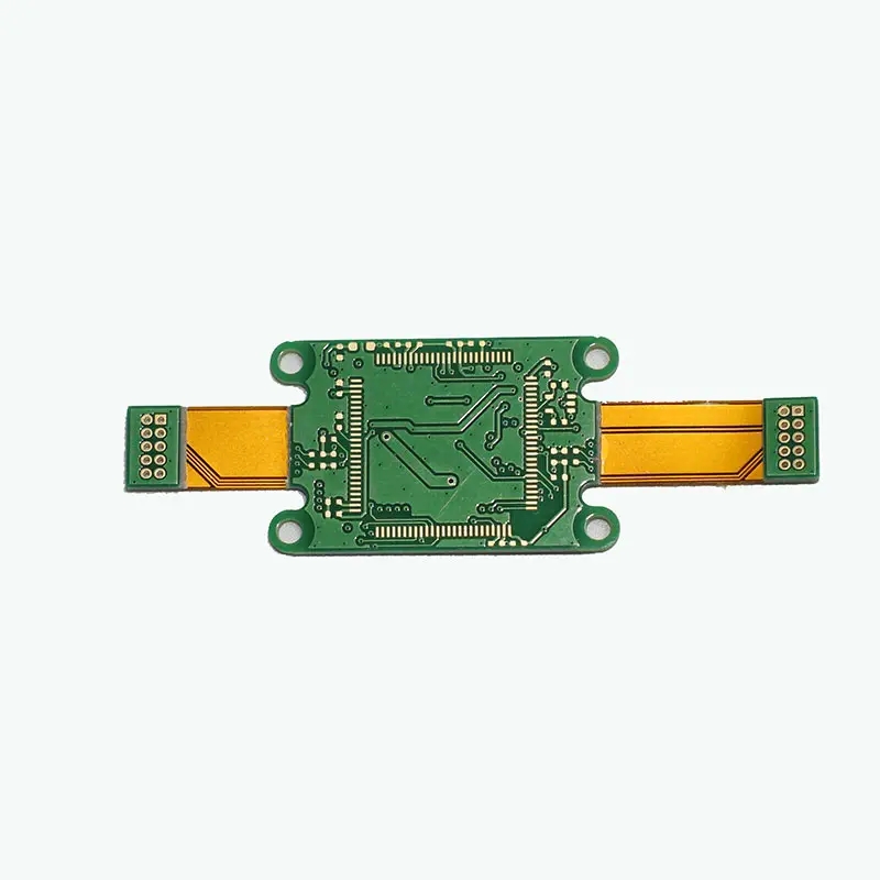
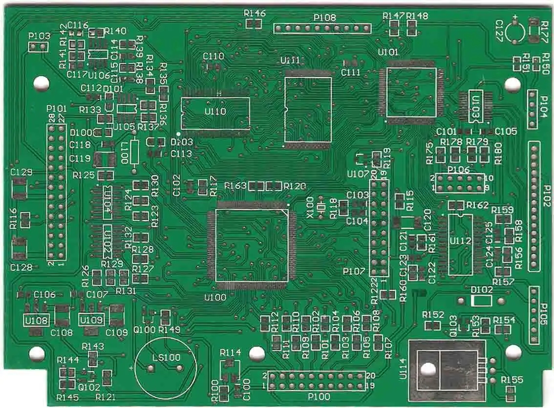
The types of SMT components are also very rich, including capacitors, resistors, inductors, diodes, transistors, ICs, connectors, crystal oscillators, screws, etc. Basically, all components can be made into SMT types. The number of MLCC capacitors on the PCBA is the largest. Due to space constraints, some capacitors are becoming smaller and smaller, from the most typical 0402 MLCC capacitor to the 01005 MLCC capacitor. Such a small resistance capacitance has high requirements for the mounting machine, reflow soldering, and the opening of the steel mesh.
ICs with various packaging forms have developed from the first commonly used SOP to QFP, QFN, etc., and then to BGA. The components go from having pins to having no pins, and the welding positions go from two sides to four sides, and then develop into tin balls at the bottom and top of the components. The number of solder joints ranges from 4 for SOP components to more than 3000 for BGA components. These changes fully show the progress of component and PCBA manufacturers in design and production process.
The SMT mounting process has also changed. At first, after printing the solder paste, red glue should be applied on the PCB, then the SMT is mounted, and finally the SMT is welded with the plug-in components through wave soldering. Up to now, there is no need to point red glue, SMT directly prints solder paste, then pastes, and then reflow soldering.
Based on the consideration of placement efficiency and quality, large PCBA generally uses several placement machines to complete the placement process. The general rule is to use a high-speed chip mounter to mount some chip components, such as resistors, capacitors, inductors, etc., and then mount crystal oscillators, transistors, LEDs, small ICs, etc. Some large components, such as BGA type IC and large connectors, such as memory slots, are arranged in the final multifunctional mounter. The number of elements selected by the tip of the mounter at one time, the placement position, etc. can be based on the performance of the mounter and the component layout of PCBA to design an optimal scheme.
The most common problems in the SMT chip production process are component inversion, misalignment, fewer parts, occasionally damaged parts, multiple parts, etc. In the NPI stage of trial production of new products, due to insufficient understanding of the polarity of product components, it is possible to have the problem of reverse polarity components in batches, such as diodes, LEDs, ICs, etc. These can be found and corrected in the FAI of the first article inspection. The offset problem can be solved by adjusting the placement coordinates, placement height, etc. When the suction nozzle of the mounter is dirty or damaged, resulting in insufficient vacuum, the problem of fewer pieces will occur. Components dropped in the middle of the journey sometimes fall onto the PCB board, causing the abnormality of multiple pieces at a certain position.
There is also a catastrophic exception, which is a damaged component. Even though the factory has many testing and inspection processes, such as AOI, online ICT, functional BFT, and manual appearance inspection, these processes cannot completely detect the damage caused by the placement process. The appearance of some damaged MLCC capacitors cannot be seen, and even their functions are normal in a short time. Only in the slicing experiment or long-term use process will show abnormalities. Excessive pressure or low height of the nozzle may cause damage to the SMD components. When the components of the same product are supplied by multiple manufacturers, special attention shall be paid to whether the component thickness of different manufacturers is different. PCB manufacturers, PCB designers and PCBA manufacturers will explain to you the advantages of SMT components.


Just upload Gerber files, BOM files and design files, and the KINGFORD team will provide a complete quotation within 24h.