
Professional PCB manufacturing and assembly
Building 6, Zone 3, Yuekang Road,Bao'an District, Shenzhen, China
+86-13410863085Mon.-Sat.08:00-20:00

Explanation of PCBA chip manufacturing process
PCBA chip processing involves a series of processing processes such as PCB manufacturing, procurement and inspection of components supplied by PCBA, SMT chip processing, DIP plug-in processing, post welding processing, program burning, PCBA testing, aging, etc. The supply chain and manufacturing chain are long. Defects in any link will lead to poor quality of a large number of PCBA boards, causing serious consequences. Therefore, the quality management of the whole PCBA chip processing process is particularly important.
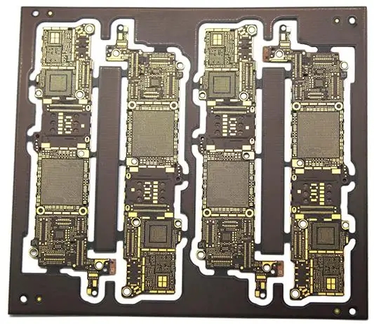
1. PCB manufacturing
It is particularly important to hold a pre production meeting after receiving the order for PCBA chip processing, mainly through the research and analysis of processing technology for PCB drawing file system, and selecting different students to submit manufacturability reports (DFM) according to the enterprise customer service needs. Many small manufacturers do not pay attention to this, which not only easily leads to poor quality of life development problems caused by poor PCB design, but also requires a lot of rework and repair work.
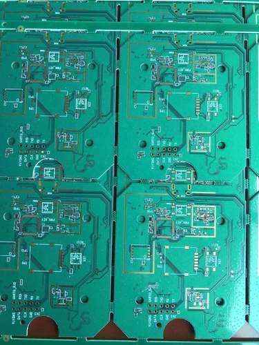
2. Procurement and inspection of components from PCBA
Strictly control the procurement channels of parts and components, obtain goods from large traders and original factories, and avoid using second-hand materials and counterfeit materials. In addition, a special PCBA incoming inspection post shall be set up to strictly inspect the following items to ensure no failure of parts.
① PCB: Check the reflow furnace temperature test to see if there is any blockage or ink leakage of the fly wire hole, and if the plate surface is bent.
② Check whether screen printing is completely consistent with typesetting, and keep constant temperature and humidity.
③ Common building materials of other enterprises: screen printing, appearance, power on measurement, etc.
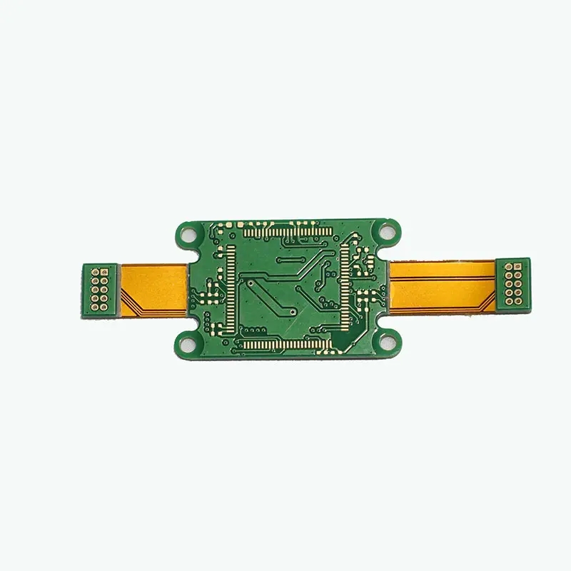
3. SMT assembly
Solder paste printing and temperature control are the key links of SMT assembly. It is necessary to use laser steel mesh with high quality requirements to meet the processing requirements. According to the requirements of PCB board, some steel meshes need to be increased or decreased, or u-shaped holes. You can make steel meshes according to the process requirements. The temperature control of the reflux furnace is critical to the paste wetting and PCBA welding, and can be adjusted according to the normal SOP operation guidelines.
In addition, strict implementation of AOI testing can greatly reduce defects caused by human factors.
4. Plug in processing
In the process of plug-in processing, the details of wave soldering die design are the key. How to use the mold base to greatly improve the yield is a process experience that PE engineers must constantly practice and summarize.
5. Program burning
In the previous DFM report, customers can be advised to set some test points (test points) on PCB to test the continuity of PCBA circuit after welding all components. If possible, you can ask the customer supplier to record the program into the main integrated circuit. You can test various touch actions more intuitively to verify the integrity of the entire PCBA function.
6. PCBA board test
For orders with PCBA testing technical requirements, the testing work mainly includes ICT (circuit system test), FCT (functional analysis test), aging test, temperature and humidity control test, drop test, etc.
PCB manufacturers, PCB designers and PCBA processors will explain a series of processes involved in PCBA chip processing.


Just upload Gerber files, BOM files and design files, and the KINGFORD team will provide a complete quotation within 24h.