
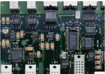
Professional PCB manufacturing and assembly
Building 6, Zone 3, Yuekang Road,Bao'an District, Shenzhen, China
+86-13410863085Mon.-Sat.08:00-20:00

Why does the PCB have an open circuit? How to improve?
PCB circuit open and short circuit is a problem that PCB manufacturers encounter almost every day, which has always plagued production and quality management personnel. The problems caused by it, such as replenishment due to insufficient shipment quantity, delivery delay, and customer complaints, are more difficult for insiders to solve. I have worked in PCB manufacturing industry for more than 20 years, mainly engaged in production management, quality management, process management and cost control. We have accumulated some experience in improving the open and short circuit problems of PCB, and now we have written a summary for discussion among peers, and we look forward to the peers who manage production and quality for reference.

First, we summarize and classify the main causes of PCB open circuit into the following aspects:
The cause analysis and improvement methods of the above phenomena are listed as follows:
1、 Open circuit caused by exposed substrate:
1. The copper clad laminate is scratched before entering the warehouse;
2. The CCL is scratched in the process of cutting;
3. The copper clad plate was scratched by the drill bit during drilling;
4. The copper clad plate is scratched in the process of transportation;
5. The copper foil on the surface was damaged due to improper operation when stacking plates after copper deposition;
6. The copper foil on the surface of the production plate is scratched when passing the leveler.
Improvement method:
1. Before PCB CCL is put into storage, IQC must carry out spot check to check whether there is scratch on the board surface and the base material is exposed. If there is, contact the supplier in time and make appropriate treatment according to the actual situation.
2. The copper clad laminate was scratched during the blanking process, mainly due to the existence of hard and sharp objects on the table of the blanking machine. During blanking, the copper foil was scratched due to the friction between the copper clad laminate and the sharp objects. Therefore, the table must be carefully cleaned before blanking to ensure that the table is smooth and free of hard and sharp objects.
3. The copper clad laminate was scratched by the drill bit when drilling, mainly because the spindle clamp bit was worn, or there were sundries in the clamp bit was not cleaned, the drill bit could not be grasped firmly, the drill bit did not reach the top, which was slightly longer than the set drill bit length, the lifting height during drilling was not enough, and the drill bit tip scratched the copper foil to form exposed substrate when the machine tool moved.
a. The clamping nozzle can be replaced by the number of times recorded by grabbing the tool or according to the wear degree of the clamping nozzle;
B. Clean the clamping nozzle regularly according to the operation procedures to ensure that there are no sundries in the clamping nozzle.
4. PCB board is scratched during transportation:
a. During handling, the number of plates lifted by the handling personnel at one time is too much and the weight is too large. The plates are not lifted during handling, but pulled up in the same way, causing friction between the plate corner and the plate surface and scratching the plate surface;
b. The boards were not placed neatly when they were put down, so they were pushed hard to rearrange them, which caused friction between boards and scratched the board surface.
5. Scratches caused by improper operation when stacking plates after copper plating and full plate electroplating:
When storing the plates after copper plating and electroplating, the plates are stacked together. When there are a certain number of plates, the weight is not small. When the plates are put down again, the plate angle is downward and there is a gravitational acceleration, forming a strong impact force hitting the plate surface, causing the plate surface to scratch and expose the substrate.
6. PCB production board is scratched when passing the leveler:
a. The baffle of the plate grinder sometimes contacts the surface of the plate. The edge of the baffle is generally uneven and there are sharp objects protruding. The plate surface is scratched when passing the plate;
b. The stainless steel transmission shaft becomes a sharp object due to damage, and the copper surface is scratched when passing the plate, exposing the base material.
To sum up, it is easy to judge the scratch and exposure of the base material after copper deposition if the line is in the form of open circuit or line gap; If the scratch on the exposed substrate occurs before copper deposition, and when it is on the line, a layer of copper is deposited after copper deposition, the copper foil thickness of the line is significantly reduced, and it is difficult to detect in the subsequent open circuit and short circuit tests. In this way, the customer may burn the line due to the inability to withstand excessive current when using, and the potential quality problems and economic losses caused are considerable.
2、 Open circuit without hole:
1. Sink copper is non porous;
2. There is oil in the hole to cause non porosity;
3. Excessive micro etching leads to non porosity;
4. Non porous due to poor electroplating;
5. The drilling nozzle burns the hole or the dust blocks the hole, resulting in non porosity.
Improvement measures:
1. Non porous copper sinking:
A. Pore free formation caused by pore forming agent: it is caused by unbalanced or ineffective chemical concentration of pore forming agent. The role of the pore forming agent is to adjust the electrical property of the insulating substrate on the pore wall, so as to facilitate the subsequent adsorption of palladium ions and ensure the complete coverage of chemical copper. If the chemical concentration of the pore forming agent is unbalanced or invalid, it will lead to non porous.
b. Activator: Its main components are pd, organic acid, stannous ion and chloride. In order to deposit metal palladium evenly on the hole wall, all parameters must be controlled to make it meet the requirements. Take our current activator as an example:
① The temperature is controlled at 35~44 ℃. If the temperature is low, the density of palladium deposition is not enough, and the chemical copper coverage is not complete; The material cost increases due to too fast reaction when the temperature is high.
② The concentration and colorimetry shall be controlled at 80%~100%. If the concentration is low, the density of palladium deposition will be insufficient and the chemical copper coverage will be incomplete; If the concentration is too high, the material cost will increase due to too fast reaction.
③ Maintain the activator solution during PCB production. If the pollution is serious, the palladium deposited on the hole wall will not be dense, and the subsequent chemical copper coverage will not be complete.
c. Accelerator: the main component is organic acid, which is used to remove stannous and chloride ion compounds adsorbed on the pore wall, revealing the catalytic metal palladium of the subsequent reaction. The chemical concentration of the accelerator we are using is controlled at 0.35-0.50N. If the concentration is high, the metal palladium is removed, resulting in incomplete chemical copper coverage. If the concentration is low, the effect of removing stannous and chloride ion compounds adsorbed on the pore wall is poor, resulting in incomplete coverage of subsequent chemical copper.
d. The control of chemical copper parameters is the key to the quality of chemical copper coverage. Take the liquid medicine parameters currently used by our company as an example:
① The temperature is controlled at 25~32 ℃, and the activity of the solution is poor due to low temperature, resulting in non porous; If the temperature exceeds 38 ℃, due to the rapid reaction of the liquid medicine and the rapid release of copper ions, it is easy to cause copper particles on the board surface to be reworked or even scrapped. At this time, the copper plating liquid medicine should be filtered immediately, otherwise the liquid medicine may be scrapped.
② The content of Cu2+is controlled at 1.5 ~ 3.0g/L, and the low content of Cu2+leads to poor activity of the solution, which will cause poor porosity; If the concentration exceeds 3.5g/L, the liquid will react quickly and release copper ions quickly, which will cause copper particles on the board surface to be reworked or even scrapped. In this way, the copper plating liquid should be filtered immediately, otherwise the liquid may be scrapped. The control of Cu2+is mainly conducted by adding copper precipitation solution A.
③ NaOH should be controlled at 10.5~13.0g/L. The low content of NaOH will lead to poor activity of the solution, which will lead to poor porosity. NaOH control is mainly controlled by adding solution B of copper precipitation. Solution B contains the stabilizer of liquid medicine. Under normal circumstances, solution A and solution B are supplemented at 1:1.
④ HCHO is controlled at 4.0~8.0g/L, and the low content of HCHO will lead to poor activity of the solution, resulting in poor porosity. If the concentration exceeds 8.0g/L, the solution will react quickly and release copper ions quickly, resulting in copper particles on the board and rework or even scrapping. In this way, the copper precipitation solution should be filtered immediately, otherwise the solution may be scrapped. HCHO control is mainly controlled by adding copper plating solution C. Solution A also contains HCHO liquid components, so when adding HCHO, first calculate the HCHO concentration increase when replenishing Solution A.
⑤ The load of copper deposition is controlled at 0.15~0.25ft2/L, which leads to poor activity of the solution and poor porosity; If the load exceeds 0.25ft2/L, the solution will react quickly and release copper ions quickly, causing copper particles on the board surface to be reworked or even scrapped. In this way, the copper plating solution should be filtered immediately, otherwise the solution may be scrapped. During production, the first cylinder plate must be towed with copper plate to activate the activity of copper plating solution, facilitate the reaction of subsequent copper plating products, ensure the density of chemical copper in the hole and improve the coverage.
Suggestion: In order to achieve the balance and stability of the above parameters, add liquid A and B to the copper sink, and configure an automatic feeder to better control the chemical components; At the same time, the automatic control device is also used to keep the temperature of the copper precipitation solution under control.
2. There is wet film oil left in the hole to cause non porosity:
a. When screen printing wet film, print a plate and scrape the screen bottom once to ensure that there is no oil accumulation on the screen bottom, and there is no residual wet film oil in the hole under normal conditions;
b. The 68~77T screen plate is used for screen printing wet film. If the wrong screen plate is used, such as ≤ 51T, wet film oil may leak into the hole, and the oil in the hole may not be clean during development, which may lead to non porosity during electroplating due to the lack of metal coating. If the mesh is high, the anti coating film may be broken by current during electroplating due to insufficient ink thickness, resulting in many metal points between circuits and even short circuits.
3. Excessive coarsening leads to non porosity:
a. If chemical roughening is used before the circuit, the temperature, concentration, roughening time and other parameters of the roughening solution should be well controlled, otherwise, non porosity may be caused due to the thin thickness of the plated hole copper and the inability to bear the copper dissolving force of the roughening solution.
b. In order to strengthen the adhesion between the coating and the base copper, the pretreatment of electroplating should be chemical roughening before electroplating. Therefore, the temperature, concentration, roughening time and other parameters of the roughening solution should be well controlled, otherwise it may also cause the problem of non porosity.
4. Non porous PCB electroplating:
a. When electroplating, when the thickness diameter ratio is large (≥ 5:1), there will be bubbles in the hole. This is because the vibration force is not enough to make the air in the hole escape, so that the ion exchange can not be realized. As a result, the hole is not plated with copper/tin. When etching, the copper in the hole is eroded, resulting in non porosity.
b. The thickness diameter ratio is large (≥ 5:1), and the oxidation phenomenon in the hole is not removed completely during the pre electroplating treatment, so the anti plating phenomenon will occur during the electroplating. The copper/tin is not plated or the copper/tin is very thin, so the anti corrosion effect cannot be achieved during the etching, which will lead to the copper in the hole being eroded away, resulting in non porosity.
5. Drilling nozzle burning or dust plugging without hole formation:
a. When drilling, the service life of the drill bit is not set properly, or the drill bit used is seriously worn, such as notch and sharpness. When drilling, the friction force is too large and the drill bit heats up, causing the hole wall to be scorched and unable to cover the chemical copper, resulting in non porosity.
b. The suction of the vacuum cleaner is not large enough, or the engineering optimization is not done well, there is dust blockage in the hole when drilling, and there is no copper deposit when chemical copper, resulting in non porosity.


Just upload Gerber files, BOM files and design files, and the KINGFORD team will provide a complete quotation within 24h.