
Professional PCB manufacturing and assembly
Building 6, Zone 3, Yuekang Road,Bao'an District, Shenzhen, China
+86-13410863085Mon.-Sat.08:00-20:00

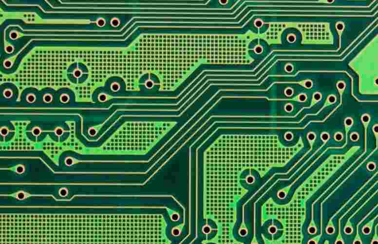
First, PCB board surface treatment
PCB board surface treatment processes include: anti-oxidation, spray tin, lead-free spray tin, sunk gold, sunk tin, sunk silver, hard gold plating, full plate gold plating, gold finger, nickel palladium OSP, etc.
The main requirements are: low cost, good weldability, harsh storage conditions, short time, environmental protection technology, good welding, smooth. Tin-spraying: tin-spraying plate is generally multi-layer (4-46 layers) high-precision PCB template, which has been used by many large communication, computer, medical equipment and aerospace enterprises and research units in China.
A gold finger is a connecting part between a memory strip and a memory slot, through which all signals are transmitted.
Goldfinger consists of a large number of golden conductive contact pieces, because the surface of the gold plated and conductive contact pieces arranged like fingers, so called "goldfinger", goldfinger plates need to be plated or sunk gold.
Goldfinger is actually coated with copper by a special process, because gold is highly resistant to oxidation and conductive. However, due to the high price of gold, most of the memory is replaced by tin, which has been popular since the 1990s.
At present, the "gold finger" of the motherboard, memory and graphics card and other devices are almost all made of tin material, only some high performance server/workstation accessories contact points will continue to use gold plating, the price is naturally expensive.
Two, the difference between gold plating and gold plating technology
Gold deposition is used by chemical deposition, through the method of chemical REDOX reaction to generate a layer of coating, generally thick, is a kind of chemical nickel gold deposit method, can reach a thicker gold layer.
Gold plating is the principle of electrolysis, also known as electroplating. Other metal surface treatment is also the majority of electroplating.
In the actual product application, 90% of the gold plate is sunk gold plate, because the poor weldability of gold-plated plate is its fatal shortcoming, but also the direct cause of many companies to abandon gold-plated process!

The plating process deposited nickel gold coating with stable color, good brightness, smooth coating and good weldability on the surface of the printed circuit. It can be basically divided into four stages: pre-treatment (oil removal, micro-etching, activation, post-leaching), nickel deposition, gold deposition, and post-treatment (waste gold water washing, DI washing, drying). The thickness of the gold deposit is between 0.025 and 0.1um.
Gold is used in circuit board surface treatment, because of the strong conductivity of gold, good oxidation resistance, long life, general application such as keyboard, gold finger plate, and the basic difference between gold plate and gold plate is that gold is hard gold (wear-resistant), gold is soft gold (not wear-resistant).
1, gold and gold plating formed by the crystal structure is not the same, gold for gold thickness is much thicker than gold plating, gold plating will be golden, more yellow than gold plating (this is one of the methods to distinguish gold plating and gold plating), gold plating will be slightly white (nickel color).
2, the crystal structure formed by gold plating and gold plating is not the same, gold plating is easier to weld, will not cause poor welding. The stress of the sunk gold plate is easier to control, which is more conducive to the processing of the bunding products. At the same time, it is because the gold is softer than the gold, so the gold plate is not wear-resistant to the gold finger (the disadvantage of the gold plate).
3. There is only nickel gold on the solder plate, and the signal transmission in the skin effect is in the copper layer, which will not affect the signal.
4, gold plating is more dense crystal structure, not easy to produce oxidation.
5, with the PCB processing precision requirements more and more high, line width, spacing has been to 0.1mm below. Gilding is easy to produce gold wire short circuit. Only the solder plate has nickel gold, so it is not easy to produce gold wire short circuit.
6. Only nickel gold is deposited on the welding plate, so the welding resistance on the line is more solid with the copper layer. The work will not affect the spacing when compensating.
7, for the higher requirements of the board, the flatness requirements are better, generally the use of gold, gold will not appear after the assembly of the black pad phenomenon. The flatness and service life of the gold plate are better than that of the gold plate.
Three, why use gold plate
As the integration of IC becomes higher and higher, the IC feet are more and more dense. The vertical tin-spraying process is difficult to flatten the thin pad, which brings difficulties to SMT mounting. In addition, the shelf life of the tin spray plate is very short.
And the gold-plated plate solves these problems:
1, for the surface mounting process, especially for 0603 and 0402 ultra-small table paste, because the flatness of the welding pad is directly related to the quality of the solder paste printing process, and plays a decisive influence on the quality of the reflow welding behind, so the whole plate gold plating in high density and ultra-small table paste process often see.
2, in the trial production stage, affected by components procurement and other factors are often not the board to immediately welding, but often have to wait for a few weeks or even months to use, the shelf life of the gold plate is many times longer than the lead tin alloy, so we are willing to use. Moreover, the cost of gold-plated PCB at the sampling stage is almost the same as that of lead-tin alloy plate.
But with more and more dense wiring, line width, spacing has reached 3-4MIL. Therefore, it brings about the problem of short circuit of gold wire: as the frequency of the signal becomes higher and higher, the signal transmission in the multi-coating caused by skin effect has more obvious influence on the quality of the signal.
Skin effect refers to: high frequency alternating current, current will tend to concentrate on the surface of the wire flow. According to calculations, skin depth is related to frequency.
Four, why the use of gold plate
In order to solve the above problems of gold-plated plate, the use of gold-plated PCB has the following characteristics:
1. Because of the different crystal structure formed by sinking gold and gold plating, sinking gold will be more yellow than gold plating, and customers are more satisfied.
2, because the crystal structure formed by gold plating and gold plating is different, gold plating is easier to weld, will not cause poor welding, cause customer complaints.
3, because the gold plate only has nickel gold on the pad, the signal transmission in the skin effect is in the copper layer will not affect the signal.
4. Because of the denser crystal structure of gold plating, it is not easy to produce oxidation.
5, because the gold plate only has nickel gold on the pad, so it will not be produced into gold wire caused by short.
Five, gold plate VS gold plate in fact, gold plating process is divided into two kinds: one is electric gold plating, one is gold plating
For the gilding process, the tin effect is greatly reduced, and the tin effect of sinking gold is better. Here, only for PCB problems, there are the following reasons:
1. In PCB printing, whether there is oil permeating film surface on PAN position, which can block the effect of tin; This can be verified by tin bleaching test.
2. Whether the PAN position meets the design requirements, that is, whether the welding pad design can ensure the support of the parts.
3, the welding pad is not contaminated, which can be obtained by ion pollution test;


Just upload Gerber files, BOM files and design files, and the KINGFORD team will provide a complete quotation within 24h.