
Professional PCB manufacturing and assembly
Building 6, Zone 3, Yuekang Road,Bao'an District, Shenzhen, China
+86-13410863085Mon.-Sat.08:00-20:00


Commercial applications utilize high frequency bandsfrom 3 MHz to more than 30 GHz. These include television, FM radio, radio astronomy, mobile phones, Wi-Fi and more. Various products in the above applications use high frequency printed circuit boards (PCBS). The low production cost of PCBS makes them attractive to modern electronic equipment manufacturers. However, in smaller quantities, the price per plate can be higher.
In order to get better, faster PCBS, designers need to pay attention to three main areas when designing boards: building materials, component interconnection, and wiring layout.
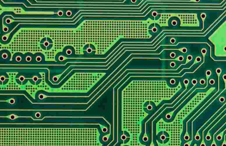
Building material
In the process of PCB design, the designer mainly considers two main characteristics of PCB material. One of them is the dielectric constant and the other is the tangent of the loss Angle. The dielectric constant affects the speed at which the signal travels through the circuit board. The tangent of the loss Angle refers to the semaphore lost due to absorption within the material. Although FR4 is a common material used to construct low-frequency circuits, more high-quality materials are needed for those using frequencies beyond 1 GHz.
Component interaction
It is important for designers of high frequency boards to consider the connection points between components and the PCB. For example, a pad placed on a ground plane can act as a capacitor. The use of surface mount devices (SMDS) can solve this problem to a large extent because of their small structural characteristics and lead length. However, as frequency increases, passive components, including SMD forms, may have non-ideal properties. Designers must take this into account and compensate for these features.
Trace layout
Once the designer has satisfactorily identified the choice of building materials and components, he/she must aim for high speed operation in a low power environment. This involves:
● Minimize vehicle noise generation
● Minimize crosstalk between routes
● Reduce the impact of ground rebound
● Impedance matching
● The correct signal cable is terminated
Minimize noise generation
Noise reduction has two main aspects. One of them is power distribution across the board, and the other involves power noise filtering.

To distribute power across the PCB, designers can use a power plane or a power bus network. Typically, the power layer on a multilayer PCB consists of two or more metal layers that carry Vcc and GND to the device. Since the power plane covers almost the entire area of the PCB, these planes have lower DC resistance. Thus, the power plane keeps Vcc levels constant while equally distributing them across all devices. It also provides noise protection, extremely high current absorption capacity and good shielding of PCB-borne signals.
An alternative to the power plane is the power bus, which consists of two or more wide metal routes that carry Vcc and GND to the device. Since this method is cheaper than power planes, two-layer PCBS often use them. When designing with a power bus network, designers need to ensure that the wiring width is as wide as possible. However, the DC resistance of the power bus network is much lower than that of the power plane.
Separating the plane and the power bus that carry the analog and digital power supplies helps minimize on-board noise generation because it prevents interaction between the two. However, an all-digital system may not have a separate analog power plane, and adding a new power plane can become prohibitively expensive unless the designer creates a partitioned island or separate plane on top of the existing layer.
While it is recommended to separate these planes between the analog and digital power supplies on the system, there may still be some unnecessary interaction between the two circuit types. The following suggestions may help reduce noise generation:
● Distribute power evenly by using separate power strips for analog power supplies. Do not use cabling or multiple signal layers to route power supplies.
● Using a ground plane near the power plane usually helps reduce the noise generated by the power supply.
● Only place the analog component on the analog grounding plane, and place the digital component on the digital grounding plane.
● Use ferrite magnetic beads to isolate analog power lines from digital power lines.
Minimize the interaction between traces
Unnecessary coupling of signals between parallel lines can lead to crosstalk. Designers minimize crosstalk by proper wiring and using microstrip and strip line layouts in layer stacking.
When forced to use two signal layers adjacent to each other, the designer minimizes crosstalk by routing all lines in one layer at an Angle to those in the next. Other techniques they employ to minimize crosstalk are minimizing the distance between the signal layer and its adjacent plane, and increasing the distance between two signal layers.


Just upload Gerber files, BOM files and design files, and the KINGFORD team will provide a complete quotation within 24h.