
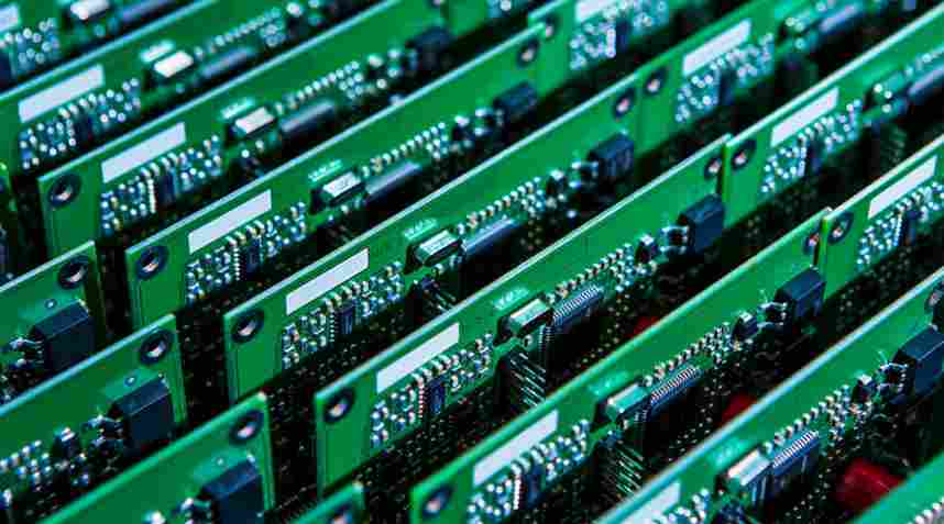
Professional PCB manufacturing and assembly
Building 6, Zone 3, Yuekang Road,Bao'an District, Shenzhen, China
+86-13410863085Mon.-Sat.08:00-20:00

PCB board copper coating 9 points of attention
The so-called copper coating, is to use the idle space on the PCB board as the base level, and then fill with solid copper, these copper areas are also known as copper filling. The significance of copper coating is to reduce the ground impedance and improve the anti-interference ability; Reduce voltage drop, improve power efficiency; Connected with the ground wire, it can also reduce the area of the loop.
Copper application needs to pay attention to those problems:
1. If the PCB is more, there were SGND, AGND, GND, and so on, is depending on the position of PCB board face, respectively to the main "to" independent copper clad as reference point, to digital and analog to separate apply copper from a few words, at the same time before the copper clad, first bold corresponding power cords: 5.0V, 3.3V and so on. In this way, multiple deformation structures of different shapes are formed.
2. For different single point connections, the practice is through 0 ohm resistance or magnetic beads or inductance connection;
3. The crystal oscillator is coated with copper. The crystal oscillator in the circuit is a high-frequency emission source. The method is to surround the crystal oscillator with copper and then ground the crystal oscillator shell separately.

4. Island (dead zone) problem, if you think it is big, then it is not much of a matter to define a hole to add.
5. At the beginning of wiring, the ground should be treated the same, when the line should be good ground, can not rely on the cover
After the copper is added through the hole to eliminate the ground pin for the connection, this effect is not good.
6. It is better not to have a sharp Angle on the PCB board (" =180 degrees "), because from the electromagnetic point of view, this constitutes a transmitting antenna! For other always have an impact on the big or small, I suggest using the edge of the arc.
7. Multilayer intermediate layer wiring open area, do not apply copper. Because it's hard to make the copper "well grounded."
8. The metals inside the device, such as metal radiators and reinforcement bars, must be well grounded.
9. The cooling metal block of the three-end voltage regulator must be well grounded. The grounding isolation belt near the crystal oscillator must be well grounded. In a word: the copper coating on PCB board, if the grounding problem is handled well, is certainly "more advantages than disadvantages", it can reduce the signal line backflow area, reduce the signal external electromagnetic interference.
What are the conventional requirements of PCB board making process
Today Xiaobian will simply introduce the routine requirements in the process of PCB board making:
1. Comply with: PCB adding process requirements
2. Surface treatment has strong antioxidant ability
3, can directly point out the shortcomings in PCB file, can be more optimized, such as packaging problems, open short circuit problems, hole plug hole cover oil problems
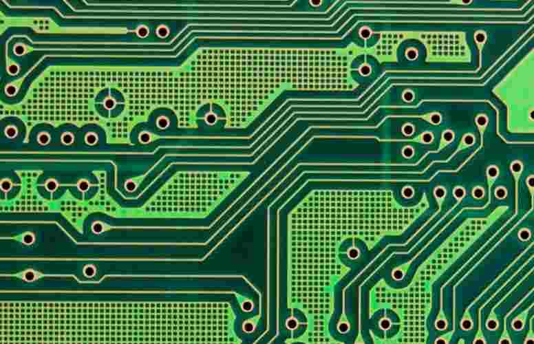
4. How to see the approximate size of the current from the PCB file, see the thickness of the line, the width of the copper, the size of the hole, the line and the copper window exposure, etc. These are the basis for identifying the size of the current
A current greater than 0.5A or above, Via size at least 0.5mm, ensure the carrying capacity
B current greater than 3A and above copper thickness requirements, generally 2OZ above, to ensure the carrying capacity
C current is greater than 4A and above thick wire and copper will generally open the window exposed copper, to ensure the carrying capacity
5, high speed signal to PCB board requirements, can run within 10GHz board
6, high speed plate impedance requirements, PP types can not be too little, better more.
A Conventional single-ended impedance is 40 ohms, 50 ohms, etc
B Conventional differential impedance is 80 ohms, 85 ohms, 90 ohms, 92 ohms, 100 ohms, etc
C plate factory can provide impedance calculation capability (with professional MI engineers).
7, the character is clear, the size deviation range is small.
8, the welding ability of the pad is strong, and it is not easy to fall off, other copper skin, line is also not easy to fall off.
9, line, hole, pad deviation precision is small, which is conducive to the structure positioning accuracy
10, line width/aperture/spacing can be more precise, the minimum line width/character 3mil, line distance/aperture 4mil, etc
11. The surface of all PCB pads is smoothed by hot air, and the smooth plate looks clean and comfortable.
12, PCB design, board, steel mesh, devices, patches can be integrated, directly PCBA to engineers for debugging, testing, verification and so on
13, the company has its own lamination recommendations, impedance requirements suggested minimum line width and line distance or recommended line width line distance, see the attachment: 4-20 layers impedance common lamination
14, the board can do the number of layers within 1-20 layers, so suitable for most customers
15. Tolerance should be as accurate and small as possible, such as plate thickness, aperture, line width, SMT, BGA, contour size, warpage, etc
16. Able to provide the company's PCB board manufacturing process and production and processing capacity requirements documents
17, the rule of the board, the board around the hope to guide the arc Angle, so that it is not easy to hurt the hand, cutting and so on
18, can add lead-free, anti-static and other environmental silk screen logo
19, can provide flight test and test report, provide impedance report


Just upload Gerber files, BOM files and design files, and the KINGFORD team will provide a complete quotation within 24h.