
Professional PCB manufacturing and assembly
Building 6, Zone 3, Yuekang Road,Bao'an District, Shenzhen, China
+86-13410863085Mon.-Sat.08:00-20:00

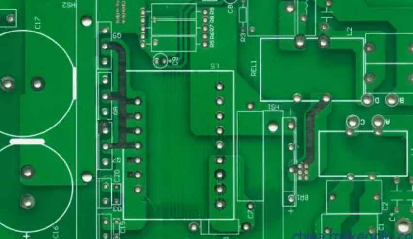
After the final product inspection is OK, the PCB board is vacuum-packed and stored for shipment. So why do PCB boards need vacuum packaging? How to store after vacuum packing? And how long does it last?
Why do PCB boards need vacuum packaging? This problem is small, but it is a lot of circuit board manufacturers attach great importance to the problem. Because once the PCB board is not sealed well, its surface gold, tin spray and solder plate parts will be oxidized and affect welding, not conducive to production. So, how to store PCB board? The circuit board is not like other products, it can not contact with air and water. First of all, the vacuum of PCB board can not be damaged. When packing, a layer of bubble film needs to be wrapped around the side of the box. The water absorption of bubble film is better, which plays a good role in moisture-proof. Then classify the emissions and label them. After sealing the box must be separated from the wall, stored away from the ground in a dry ventilated place, but also avoid sunlight. The temperature of the warehouse is best controlled at 23±3℃, 55±10%RH, under such conditions, the surface treatment of gold, electric gold, tin spray, silver plating PCB board can be stored for 6 months, the surface treatment of silver, tin, OSP PCB board can be stored for 3 months. For the PCB board that is not used for a long time, the circuit board manufacturer had better brush a layer of three anti-paint on it. The role of three anti-paint can be moisture-proof, dustproof and anti-oxidation. This will increase the PCB board storage life to 9 months.
An example of PCB multilayer plate illustrates the mechanism of plasma processing
Plasma refers to light like purple light, neon light, also known as the fourth phase of sheet matter. The plasma phase is a state of disorderly motion of excited electrons and molecules in atoms, so it has quite high energy.
(1) Mechanism:
When energy (such as electric energy) is applied to gas molecules in the vacuum chamber, the shock of accelerating electrons causes the outermost electrons of molecules and atoms to be excited and generate ions, or highly reactive free radicals.
The ions and free radicals generated in this way are accelerated by continuous collision and electric field force, so that they collide with the surface of the material, and destroy the molecular bonds within a few microns, resulting in the reduction of a certain thickness and the formation of concave and convex surface. At the same time, physical and chemical changes are formed on the surface of the functional groups of the gas composition, so as to improve the bonding force of copper plating, pollution removal and other plate loading effects.

The gases commonly used for plasma treatment are oxygen, nitrogen and carbon tetrafluoride gas. The following is an example of the mechanism of plasma treatment by using a gas mixture consisting of oxygen and carbon tetrafluoride gas:
(2) Purpose:
1, concave/hole wall resin stain;
2, improve the surface wettability (PTFE surface activation treatment);
3, using laser drilling of blind hole carbon treatment;
4, change the inner layer surface morphology and wettability, improve the interlayer binding force;
5. Remove residuals of resist and welding resistance film.
(3) Examples:
A. Activation of pure polytetrafluoroethylene materials
For the activation treatment of pure polytetrafluoroethylene material, a single step activation through hole process is used. The gas used is mostly a combination of hydrogen and nitrogen.
The plates to be treated do not need to be heated because the teflon is treated to become active and the wettability is increased. Once the vacuum chamber reaches operating pressure, start working gas and RF power supply.
Most pure teflon sheets are processed in about 20 minutes. However, due to the restorative properties of the PTFE material (return to a non-wetting surface state), the metallization of the chemical-deposited copper holes needs to be completed within 48 hours after plasma treatment.
B. Activation of PTFE materials containing fillers
For printed circuit boards made of PTFE materials containing fillers (e.g. irregular glass microfibres, glass braided reinforced and ceramic filled PTFE composites), a two-step process is required.
The first step is cleaning and microetching the filler. Typical operating gases in this step are carbon tetrafluoride gas, oxygen and nitrogen.
The second step is equivalent to the one-step plate copying process used in the surface activation treatment of pure PTFE materials mentioned above.


Just upload Gerber files, BOM files and design files, and the KINGFORD team will provide a complete quotation within 24h.