
Professional PCB manufacturing and assembly
Building 6, Zone 3, Yuekang Road,Bao'an District, Shenzhen, China
+86-13410863085Mon.-Sat.08:00-20:00

I. Definition of HDI board:
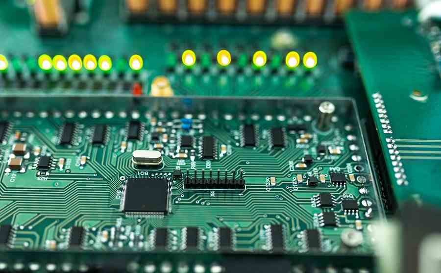
High Density Interconnection (HDI) High density interconnection (HDI) is the Chinese term for high-density interconnection, which is usually characterized by high density of lines, thinner than common PCB board lines, and the presence of microholes (commonly known as blind holes, aperture < 125um) multilayer high precision printed circuit board. HDI overlay commonly known as the circuit board laminated laminated pattern diagram, also known as the mechanism diagram. Usually the same number of layers of circuit boards, and different stacking, through the process will be different.
Usually, the industry calls the number of HDI passing through the laser as the order, the one passing through is called the first order, also called the PULLS I, and the two passing through is called the second order, also called the PULLS II. And so on.
Two, the layer increase method in the HDI board:
The so-called build-up circuit board is printed a HDI circuit board composed of a layer by layer by overlapping method to form a three-degree spatial structure. The circuit board formed by the additive layer method can effectively improve the circuit board because the plug hole density between the upper and lower circuits is much higher than that of the traditional printed circuit board.
Actually increases the layer of the concept is not new technology, in the early 1970 s development of semiconductor process technology, have begun to use new layer method in the concept of silicon wafer is formed on aluminum wires and polyurethane 橀 amine such as insulating layer of multilayer layer structure.
Now, the concept of additive layer method has been introduced into the substrate used in current chip packaging technology. Since its development in the 1970s, chip packaging modules in large computers have used layer-on circuit boards that form copper wires and polyimide insulation on a ceramic substrate. An additional insulating layer is provided on the ceramic substrate, and the lines above and below the insulating layer can be channeled through the plug holes and encapsulated the wafer to the substrate in the form of crystal coating. The region around the wafer has an enhanced circuit of copper and polyimide. The thermal conduction module is a typical example of high density added layer HDI circuit board.
Theer, Position coordination accuracy of HDI board:
In addition to the precision of the size of the circuit board, the biggest technical issue of the circuit production is the precision of the position coordination. Because high density HDI boards must be assembled with high density components, these encryption actions make the board each relative geometry more difficult to match. For example, the position produced after drilling must be matched with the exposure of the line, and the image of the stop welding paint must be matched with the image of the line. These collocation actions are positional accuracy problems in circuit board production, but also important technical problems in the production of high density HDI circuit boards.
Four, the influence of HDI board on accuracy:
In general, the substrate itself is an important determinant of position accuracy. Because the circuit board material, itself is a mixture of materials. Especially the resin material of the main body, it will vary with temperature, barbecue time, humidity and so on. In addition, in the process of processing, if you have to do extended machining, so the variation of size will be greater. However, the problem of location collocation has always existed in the production of substrate, when the through hole is produced, it must still go through various wet process processing, in order to achieve the conductivity function of the hole. In the process of line etching, most of the accumulated stress in the previous process will be released. If a special process is used and barbecue must be added, then the overall variation will be more.
five. Impact of film on accuracy:
As for the negative, no matter what kind of material and form of negative is used, the current production method of most circuit boards is still the use of flat plate contact production, negative will be another factor that has to be discussed. Most of the film film because the dimensional stability is indeed poor, in the high precision substrate products almost can not be used. But for some small quantity can not care about the high efficiency of the substrate, there are also some producers use smaller substrate size to overcome the problem of counterpoint. For the majority of mass producers, how to make use of large size counterpoint production mode is still an important technical issue of thin wire substrate manufacturing.
Six. Impact of tools and materials on accuracy:
For the accuracy and stability of production tools and materials, controlling the source of material acquisition will be an important control matter. This includes the supplier's material manufacturing stability, quality control ability, type of materials used, grade of manufacturing machinery, clarity, polymerization stability, etc. Many factors will affect the subsequent size changes of tools and materials. This is especially the selection of substrate, must pay special attention to the supply of fiber cloth quality stability, substrate manufacturers coating and operation control ability of stability, compression completed substrate plate dimensional stability. These problems often occur outside the substrate manufacturer, and there is little room for improvement once the material reaches the production line.
Basically, there are only two important materials for the simple analysis of the position itself. One is that the stability of the production tools and product size must be high, otherwise the variation will make the difference produce random changes, and there is no possibility of size matching. The second is the alignment procedure in the alignment process, which generally represents the handling ability of the exposure machine.
In the mechanical counterpoint part, since the majority of counterpoint accuracy comes almost entirely from the counterpoint system's control capabilities, the producer must have a thorough understanding of the counterpoint capabilities of the exposure system used. At present, most of the exposure systems commonly used for loading plates use four target alignment systems to improve the overall fit.
At present, most automatic exposure systems use a solid-state camera to read the target image of the negative and substrate, and then calculate the difference as the basis for position correction. In terms of mechanical design, the method of moving and static is adopted, which can be film moving or substrate moving. As long as the operation accuracy and control are good, there is no real difference between good and bad. The precision of alignment can be set, generally according to the allowable tolerance of the design line when the index is set. Most current alignment systems are built in a specification setting mode, which means exposure can be made whenever the tolerance falls within the specification. But the actual ideal demand should be to achieve the best degree of alignment, that is, alignment deviation uniformity, which requires the efforts of mechanical manufacturers.


Just upload Gerber files, BOM files and design files, and the KINGFORD team will provide a complete quotation within 24h.