
Professional PCB manufacturing and assembly
Building 6, Zone 3, Yuekang Road,Bao'an District, Shenzhen, China
+86-13410863085Mon.-Sat.08:00-20:00

With the continuous development of electronic science and technology, PCB technology has also undergone great changes, and the manufacturing process also needs to progress. At the same time, the process requirements of PCB circuit boards in each industry have gradually improved. For example, gold and copper are used in the circuit boards of mobile phones and computers. As a result, the pros and cons of the circuit boards have gradually become easier to distinguish.
Take you to understand the surface process of PCB board, compare the advantages and disadvantages of different PCB board surface treatment process and applicable scenarios.
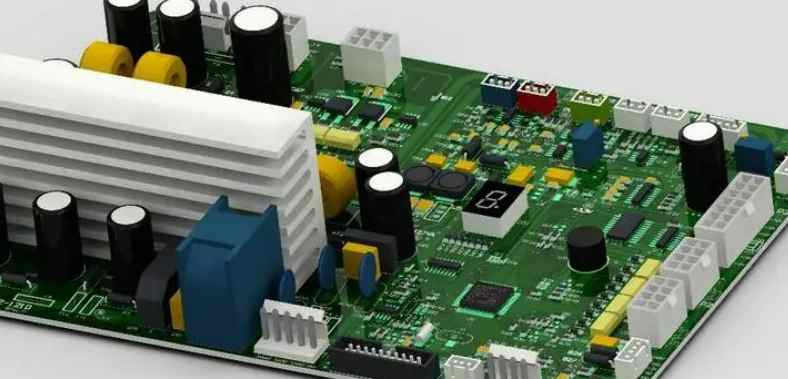
Pure from the appearance, the outer layer of the circuit board has three main colors: gold, silver, light red. According to the price classification: gold is the most expensive, silver is second, light red is the cheapest, from the color is actually easy to judge whether the hardware manufacturers have jerry-cutting behavior. But the circuit board inside the line is mainly pure copper, that is, bare copper plate.

One, bare copper plate
The pros and cons are obvious:
Advantages: Low cost, flat surface, good weldability (without being oxidized).
Disadvantages: easy to be affected by acid and humidity, can not be put for a long time, after unpacking need to be used up within 2 hours, because copper exposed to the air easy oxidation; Cannot be used on double panels because the second side is oxidized after the first reflow welding. If there is a test point, solder paste must be printed to prevent oxidation, otherwise there will be no good follow-up contact with the probe.
Pure copper if exposed to air is easily oxidized, the outer layer must have the above protective layer. And some people think that gold is copper, which is wrong because it's the protective layer on top of copper. So you need a large area of gold plating on the circuit board, that is, I took you to understand before the gold plating process.
Two, gold-plated plate
Gold is real gold. Even a thin coating can account for nearly 10% of the board's cost. In Shenzhen, there are many businessmen specializing in the acquisition of scrap circuit boards, through certain means to wash out gold, is a good income.
The use of gold as a coating, one is to facilitate welding, two is to prevent corrosion. Even the gold finger of a memory that has been used for several years is still shining. If copper, aluminum and iron had been used, they would now be rusted into a heap of scrap.
Gold coating is widely used in the parts of the circuit board welding pad, gold finger, connector shrapnel and other positions. If you find that the circuit board is actually silver, then needless to say, call the consumer rights hotline, must be the manufacturer, not the proper use of materials, using other metal to fool customers. The most widely used mobile phone circuit board motherboard is mostly gold plate, gold plate, computer motherboard, audio and small digital circuit board are generally not gold plate.
The advantages and disadvantages of the gold-sinking process are not difficult to figure out:
Advantages: It is not easy to oxidize, can be stored for a long time, the surface is smooth, suitable for welding fine clearance pin and small solder joint components. Preferred PCB board with keys (such as mobile phone board). It can be repeated multiple times without much loss of weldability. It can be used as the base material for COB(ChipOnBoard) batting line.
Disadvantages: High cost, poor welding strength, because of the use of nickel plating process, prone to black disk problems. The nickel layer oxidizes over time, and long-term reliability is an issue.
Disadvantages: Susceptible to acid and humidity. When used for secondary reflow welding, it should be completed within a certain time, usually the second reflow welding effect will be poor. If it lasts longer than three months, it must be resurfaced. It should be used within 24 hours after unpacking. OSP is the insulating layer, so the test point must be printed with solder paste to remove the original OSP layer before it can contact the pin point for electrical testing.
The only function of this organic film is to ensure that the inner copper foil does not oxidize before welding. The film evaporates when you heat it up during welding. The solder will be able to weld the copper wire and components together.
But it is very corrosion resistant, an OSP circuit board, exposed to the air for more than ten days, can not be welded components.
Many computer motherboards use the OSP process. Because the board area is too large to use gold plating.


Just upload Gerber files, BOM files and design files, and the KINGFORD team will provide a complete quotation within 24h.