
Professional PCB manufacturing and assembly
Building 6, Zone 3, Yuekang Road,Bao'an District, Shenzhen, China
+86-13410863085Mon.-Sat.08:00-20:00

What should be checked after PCB design? PCB design manufacturability
The design of printed circuit board is based on the circuit schematic diagram to realize the functions required by the circuit designer. The design of printed circuit board mainly refers to layout design, which needs to consider the layout of external connections. The optimal layout of internal electronic components, the optimal layout of metal wiring and through-hole, electromagnetic protection, heat dissipation and other factors. Excellent layout design can save production costs and achieve good circuit performance and heat dissipation. Simple layout design can be realized by hand, while complex layout design needs to be realized by computer aided design (CAD)
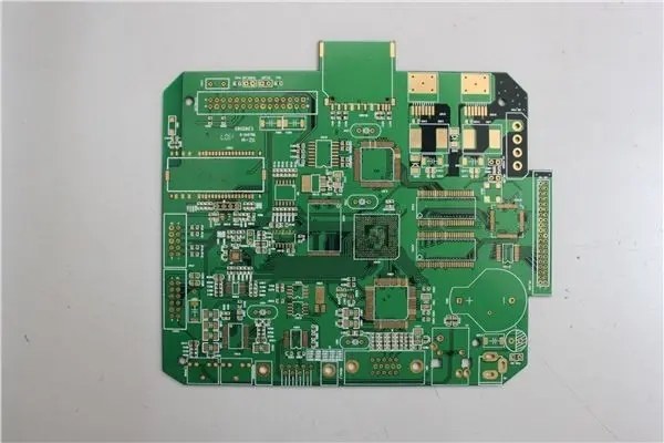
With the intellectualization of people's life, many things are also developing towards the direction of intellectualization, which requires more circuit boards to achieve. PCB design is the basis, and the manufacturability of PCB can ensure the next step. After PCB design, we need to check the function of all items. Just like we finish the examination paper ourselves, we should do a simple analysis and recheck all problems to ensure that we will not make big mistakes due to negligence. Similarly, PCB design is the same. The PCBA manufacturer will introduce what items need to be checked after PCB design.
The following items need to be checked after PCB design:
DFM review of optical board: whether the production of optical board meets the technical requirements of PCB manufacturing, including line width, spacing, wiring, layout, through-hole, marking, wave soldering component direction, etc.
2. Check the consistency between the actual components and the bonding pad: whether the actual SMT mounting components purchased are consistent with the designed bonding pad (if not, please use a red label to indicate), and whether they meet the spacing requirements of the SMT mounting machine.
3. Generate 3D graphics: generate 3D graphics, check whether space elements interfere with each other, whether element layout is reasonable, whether it is conducive to heat dissipation, whether it is conducive to SMT reflow soldering heat absorption, etc.
4. PCBA production line optimization: optimize the loading sequence and the location of the material station. Input the existing pasting machine (such as Samsung high-speed machine, universal multi-function machine) into the software, and distribute the components to be pasted to the existing board. How many pasting methods does Samsung have, how many pasting methods do Samsung have in the world, how many locations and where to pick up materials, etc. This can optimize the SMT chip processing program and save time. For multi line production, the distribution of installed components can also be optimized.
5. Operation instructions: automatically generate the operation instructions of the workers on the production line.
6. Revision of Inspection Rules: inspection rules can be modified. For example, if the component spacing is 0.1mm, the manufacturer and circuit board complexity can be set to 0.2mm according to the specific model, the line width is 6mi, and it can be changed to 5mil in high-density design.
7. Support Panasonic, Fuji and Universal patch software: it can automatically generate paste software to save programming time.
8. Automatically generate steel plate optimization graphics.
9. Automatically generate AOI and X-ray programs.
10. Check to support multiple software formats (Japan, KATENCE, China PROTEL).
11. Check the BOM and correct relevant errors, such as spelling errors of the manufacturer. BOM is converted to software format.
The above is my introduction to "What needs to be checked after PCB design? Manufacturability of PCB design", providing you with a reference. I wish you a happy life!


Just upload Gerber files, BOM files and design files, and the KINGFORD team will provide a complete quotation within 24h.