
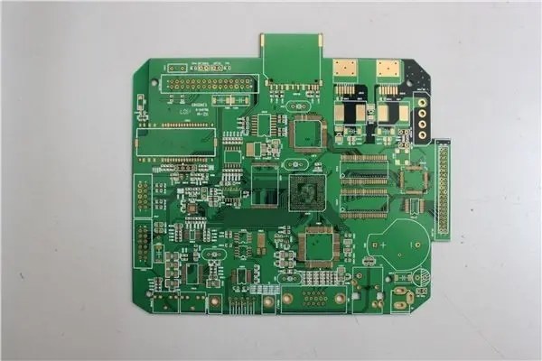
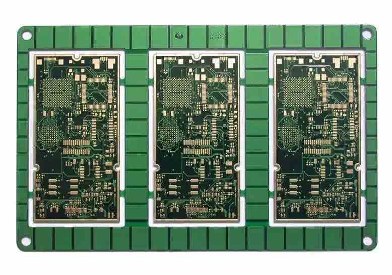
Professional PCB manufacturing and assembly
Building 6, Zone 3, Yuekang Road,Bao'an District, Shenzhen, China
+86-13410863085Mon.-Sat.08:00-20:00


What are the PCB design software? What are the steps of PCB design?
PCB design is also called PCB design, because the full name of PCB (also called printed circuit board) in English is Printed circuit board, abbreviated as PCB, so PCB design is also called PCB design; PCB design, from manual drawing to more and more large-scale component library, has powerful automatic layout and routing functions, which is more and more convenient for our engineers to design PCB. Next, I would like to introduce to you what are the PCB design software? What are the steps of PCB design?
1、 What are the PCB design software?
1. In China, protel, protel 99se, protel DXP, Altium are the software that a company develops and continuously upgrades; The current version of Altium Designer 15 is relatively simple and random in design, but it is not very good to make complex PCBs.
2. Cadence spb software Cadence spb This is Cadence software. The current version is Cadence SPB 16.5; The ORCAD schematic design is an international standard; Among them, PCB design and simulation are complete, which is more complex than protel in use, mainly because of complex requirements and settings; However, it has made provisions for the design, so it can achieve twice the result with half the effort. It is obviously stronger than protel.
3. Mentor's BORDSTATION and EE, in which BOARDSTATION is only applicable to UNIX system and not designed for PC, so fewer people use it; The current Mentor EE version is Mentor EE 7.9 and Cadence spb, which belong to the same level of PCB design software. In some places, Mentor EE is inferior to cadence spb. Its strengths are stay wire and flying wire, known as the flying wire king.
4. EAGLE Layout This is the most widely used PCB design software in Europe. The PCB design software mentioned above is widely used, and Cadence spb and MentorEE are the rightful kings. If you are a beginner in PCB design, I think Cadence spb is better. It can develop a good design habit for designers and ensure good design quality. What are the circuit board design software explained by the circuit board assembly and circuit board processing manufacturers? What are the steps of PCB design?
2、 What are the steps of PCB design?
1. Layout design
In PCB, special components refer to the key components in the high-frequency part, the core components in the circuit, the components susceptible to interference, the components with high voltage, the components with high heat, and some heterosexual components. The positions of these special components need to be carefully analyzed, and the tape layout should meet the requirements of circuit functions and production requirements. Improper placement of them may cause circuit compatibility problems and signal integrity problems, which may lead to PCB design failure.
The size of PCB shall be considered first when placing special components in the design. Quick buy points out that when pcb size is too large, the printing line is long, the impedance increases, the dry resistance decreases, and the cost increases; If it is too small, the heat dissipation is poor, and adjacent lines are easily disturbed. After determining the size of PCB, determine the swing position of special components. Finally, all components of the circuit are arranged according to the functional unit. The location of special components shall generally comply with the following principles:
(1) Shorten the connection between high-frequency components as much as possible, and try to reduce their distribution parameters and mutual electromagnetic interference. Components susceptible to interference shall not be too close to each other, and the input and output shall be as far away as possible.
(2) Some components or wires may have high potential difference, so their distance shall be increased to avoid accidental short circuit caused by discharge. High voltage components should be kept out of reach.
(3) Components weighing more than 15G can be fixed with brackets and then welded. Those heavy and hot components should not be placed on the circuit board, but on the bottom plate of the main box, and heat dissipation should be considered. Thermal components shall be far away from heating components.
(4) For the layout of adjustable components such as potentiometers, adjustable inductance coils, variable capacitors, microswitches, etc., the structural requirements of the whole board should be considered. Some switches that are often used should be placed in places that are easy to reach when the structure allows. The layout of components should be balanced, and the density should be appropriate.
For the success of a product, the first is to pay attention to the internal quality. The second is to give consideration to the overall beauty. Only a perfect board can become a successful product.
1. Placing sequence
(1) Place components closely matching with the structure, such as power socket, indicator light, switch, connector, etc.
(2) Place special components, such as large components, heavy components, heating components, transformers, ICs, etc.
(3) Place small components.
1. Layout inspection
(1) Whether the size of the circuit board is consistent with the processing size required by the drawing.
(2) Whether the layout of components is balanced, orderly arranged and completely distributed.
(3) Whether there are conflicts at all levels. For example, whether the components, frames, and layers requiring silk screen are reasonable.
(4) Whether the commonly used components are convenient for use. Such as switches, plug-in devices, components that must be replaced frequently, etc.
(5) Whether the distance between thermal components and heating components is reasonable.
(6) Whether the heat dissipation is good.
(7) Whether the interference of the line needs to be considered.
The above is my opinion on "What are the PCB design software? What are the steps of PCB design?" The introduction of, provide for everyone to refer to, wish everyone a happy life!


Just upload Gerber files, BOM files and design files, and the KINGFORD team will provide a complete quotation within 24h.