
Professional PCB manufacturing and assembly
Building 6, Zone 3, Yuekang Road,Bao'an District, Shenzhen, China
+86-13410863085Mon.-Sat.08:00-20:00

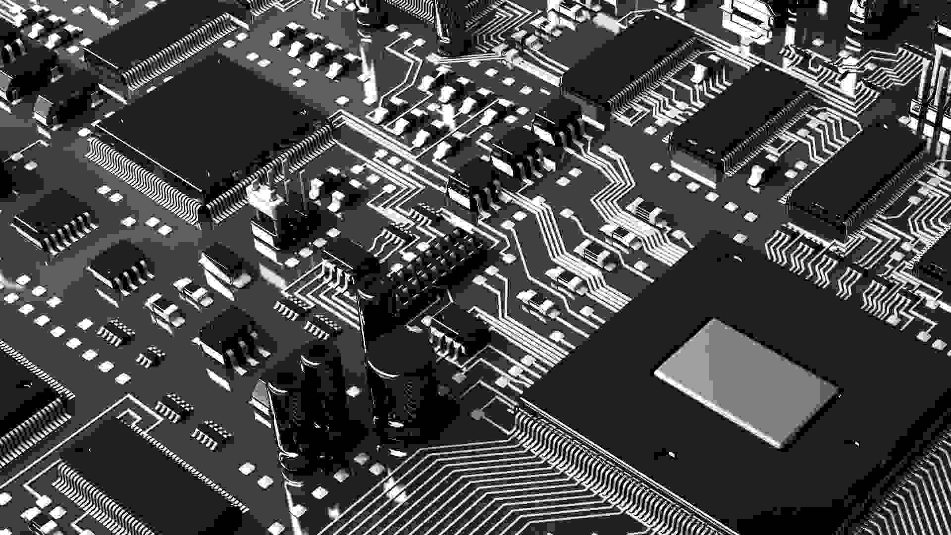
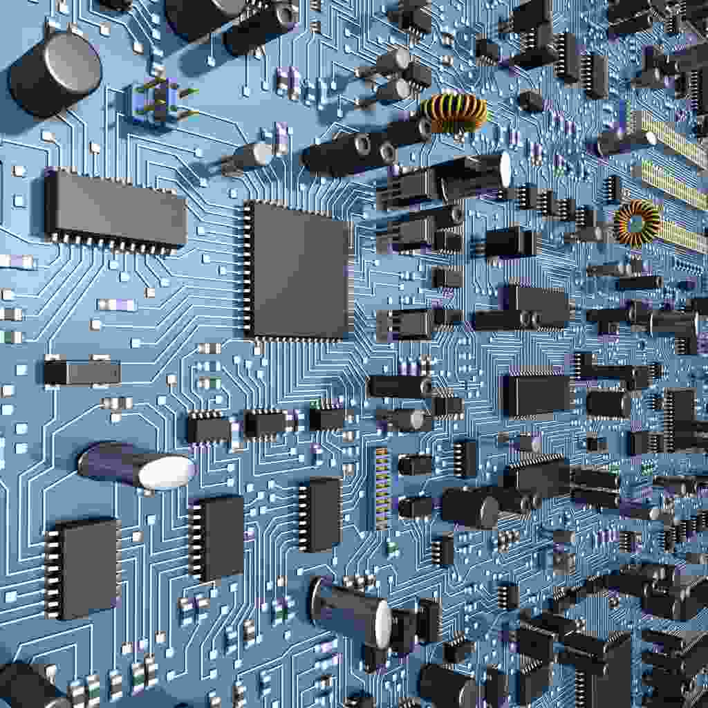
Top level PCB surface treatment of PCBA and which one to use
Details of PCB surface treatment
In the purchase step of product development, the surface treatment of PCB on bare board seems to be a trivial decision, but understanding the changes and complexity may prevent problems.
The surface finish of printed circuit board mainly does two things. First, it helps protect copper circuits from corrosion. Second, it creates weldable surfaces for your PCBA components. Therefore, the following items need to be considered:
What components are you using
Expected output of your PCB boards
Requirements of circuit board for environment and general durability
Impact on the environment
budget
The five most common types of PCB surface treatment and their advantages and disadvantages will be discussed below.
Hot air solder leveling (HASL)
The most commonly used PCB surface finish is HASL or "hot air solder leveling". This is because it always exists and is the most economical. However, even if the price is not close to HASL, the new technology can still make the surface finish higher.
In this process, the PCB board is immersed in the molten solder, and then leveled with a hot air knife, hence the name. If your circuit board uses through holes or large SMT components, HASL can work properly. However, if your circuit board uses SMT components smaller than 0805 or SOIC, it may not be an ideal surface treatment.
This surface finish is not completely flat and may cause problems with smaller components. The solder used in this process is usually tin lead. This means that it is also not RoHS compliant. If your project requires RoHS or your company wants to reduce the amount of lead used, you may need to specify a lead-free HASL.
advantage:
Excellent solderability
Cheap/low cost
Allow large processing windows
Rich industry experience/popularity
Disadvantages:
Non flat surface and difference in thickness/morphology between large and small pads
Not suitable for smaller and denser components (SMD and BGA with spacing less than 20 million)
Fine pitch bridging
Not suitable for HDI products
Lead free HASL
Lead free HASL is similar to conventional HASL, but tin lead solder is not used.
In contrast, lead-free HASL uses tin copper, tin nickel or tin copper nickel germanium in its process. This makes lead-free HASL an economical and RoHS compliant option. However, similar to standard HASL, it does not apply to smaller SMT components.
The use of immersion coatings can make better use of PCBA for high-density/fine pitch components. Sometimes the price is a little higher, but they are more suitable for this purpose and can reduce problems in the production process.
advantage:
Excellent solderability
Cheap/low cost
Allow large processing windows
Rich industry experience/popularity
Many hot outings
Disadvantages:
Non flat surface and difference in thickness/morphology between large and small pads
High treatment temperature in the range of 260-270 ° C
Not suitable for smaller and denser components (SMD and BGA with spacing less than 20 million)
May bridge on fine pitch
Tin dipping (ISn)
In ISn PCB manufacturing, chemical process is adopted.
This process requires depositing a flat metal layer onto the copper wire. The flatness of the coating makes it suitable for small parts. Tin is one of the most economical types of immersion coatings. Although this is a budget friendly option, it also has some disadvantages.
The biggest problem is that tin begins to tarnish when it is deposited on copper. Therefore, if you want to avoid low-quality solder joints, you need to weld the components within 30 days.
In mass production, this may not be a problem. If you run out of a large number of circuit boards soon, you can also avoid tarnishing. However, if the output is low or the stock of bare boards is to be kept, it may be wiser to use coatings such as silver dipping.
advantage:
Flat welding area
Suitable for small pitch/BGA/smaller components
Reasonable price of lead-free surface treatment
Suitable surface treatment for press fit
Good weldability even after multiple thermal cycles
Disadvantages:
Sensitive to operation – gloves should be worn
Tin whisker problem
Erosion of welding resistance layer - the dam of welding resistance layer shall be ≥ 5 mil
Baking before use will reduce solderability
Silver Immersion (IAg)
Therefore, on the one hand, immersion silver does not react with copper as ISn does. On the other hand, it loses its luster when exposed to air. Therefore, all IAg PCBs should be stored in rust proof packaging during storage and handling.
After these PCBs are properly packaged, they can be reliably welded for 6 to 12 months. However, once the PCB board is taken out of its package, it will need to be reflowed within one day. Gold plating can extend the shelf life.
advantage:
Flat surface
Ideal for small size, small spacing and BGA components
Medium price lead-free surface treatment
The board can be reworked
Disadvantages:
Possible handling/fading problems
Special packaging to prevent discoloration
Small window for optimal weldability during assembly
Electroless nickel gold plating (ENIG)
My personal favorite PCB surface treatment is ENIG. The method of electroplating gold is to use a thin layer of gold on chemical nickel or electrolytic nickel.
Gold plating is hard and durable. This can make it have a long shelf life, even a good manufacturer can last for several years. Materials, processes and reliability often make ENIG boards more expensive than other surface treatment boards. However, we have seen that many boards of directors have begun to transfer most of the processes to ENIG. Even if the price difference between them and other institutions is small, the price is the same.
advantage:
Flattest surface finish
Suitable for small size, small spacing and BGA components
Reliable manufacturing processes and procedures
Lead wire bonding
Disadvantages:
Sometimes more expensive to complete
BGA's black mat problem
Loss of Signal (RF)
It is better to avoid using BGA defined by solder mask
Select the appropriate PCB surface treatment for your project
The surface finish of PCB is a crucial decision and should be considered before manufacturing. It is important to consider things such as component type and output for a smooth assembly process. Durability, environmental impact and cost may also be factors to consider and discuss with your team. By fully understanding your needs, you can only select the appropriate surface finish for PCB. The PCB processing factory explains the top PCB surface treatment of PCBA, which type to use, and the details of PCB surface treatment.


Just upload Gerber files, BOM files and design files, and the KINGFORD team will provide a complete quotation within 24h.