
Professional PCB manufacturing and assembly
Building 6, Zone 3, Yuekang Road,Bao'an District, Shenzhen, China
+86-13410863085Mon.-Sat.08:00-20:00

Engineers share the reason of PCBA and PCB component warping
Warpage in PCB and PCBA
Did you notice that certain plates are no longer flat after assembly? Or is the bare board you received not completely flush? PCB warping is a general term used to describe the irregular PCB shape, independent of the shape itself (bending, bending, twisting, etc.). A major struggle is that during the welding cycle, a plate may transition from flat to warped, so it cannot always be grasped by hand. Therefore, the original shape may not be directly related to the shape after PCB welding. Warpage in PCB and PCBA can cause problems during assembly or final implementation. We will discuss in depth the reasons for these two situations and how to prevent this problem.
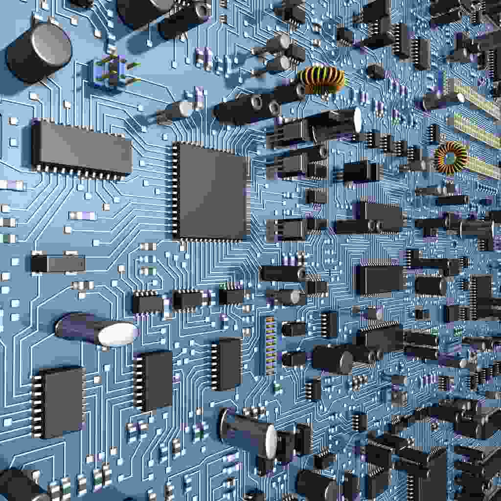
PCB warping
When the exposed PCB is filled, it enters the picker, which places components on top of it to prepare for the welding process. When using warped plates, such unevenness may lead to improper placement or parts falling. When the circuit board passes through the reflow furnace, flatness is also important. These machines heat the plates to a high temperature, which may change the material and warp the plates. This may also lead to parts slipping, incorrect placement, welding bridges or other welding problems.
PCB warping will lead to poor quality and low acceptability of the final product. Ensuring the flatness of the circuit board is essential to prevent assembly related problems, including bridging or open connectors, which can eventually lead to product failure.
Causes and Prevention of PCB Warpage
PCB is composed of different substrate layers that allow voltage and signal to pass through. The processing workshop uses many materials suitable for our industry. These materials have good thermal stability, anti ion mobility, low dielectric constant, good processability and no substrate drift. The current PCB manufacturing technology can ensure that the PCB warpage remains less than 0.5% in all states during PCB assembly.
The welding process may be the largest catalyst for plate warping. In reflow furnace or wave soldering machine, PCB is exposed to high temperature, which causes material on the board to expand and contract. Due to the difference between the expansion coefficient of copper and the base material, there may be unequal expansion and contraction between the two, resulting in the generation of internal stress. As a result, the plate may warp as it cools and stabilizes to its resting state. Incorrect storage and handling may also cause warping. If the board absorbs moisture, it may cause the area to heat and cool at different rates, resulting in warping.
Other factors that may cause plate warping may be actual design. In the design process, the engineer must consider the balance between the circuit area and the conductor pattern, as well as the symmetry of the circuit board stack. If the operating temperature of the PCB exceeds the rated temperature, it may also play a role. Finally, during the PCB manufacturing process, PCB products experienced several thermal drifts and heat treatments. When the treatment temperature exceeds the Tg of the copper clad laminate, the manufacturer must heat both sides of the substrate evenly and evenly, while keeping the treatment time as short as possible to reduce the warpage of the substrate.
Conclusion on warped PCB
Bent PCBs can cause problems in picking and placing assemblies. The SMT assembly will not fall on the expected pad, the assembly will not enter the expected hole on the board, the assembly may slip, or the solder may bridge and short circuit. Irregular PCBA is difficult to install into the chassis, and may cause reliability problems on site. All this makes it very important that all stakeholders do their best to avoid PCB warping. To eliminate this problem, please ensure that the circuit boards are manufactured from high-quality stores, and the warehouse should pay attention to the handling and storage of circuit boards, especially in wet places. In addition, engineers can pay attention to the design to ensure the balance plate, or they can specify higher Tg materials to better make the plate bear different stresses. The circuit board processing factory explained that the engineers shared the causes of PCBA and PCB component warpage, and the solutions to PCB and PCBA warpage.


Just upload Gerber files, BOM files and design files, and the KINGFORD team will provide a complete quotation within 24h.