Professional PCB manufacturing and assembly
Building 6, Zone 3, Yuekang Road,Bao'an District, Shenzhen, China
+86-13923401642Mon.-Sat.08:00-20:00
Information

Information

Four suggestions for PCB design from the point of view of drawing board
18Jun
Caddy 0 Comments

Four suggestions for PCB design from the point of view of drawing board

t present, in PCBA processing, the introduction of advanced testing equipment for quality control of...

Why can't the signal line be changed multiple times in high-speed PCB design?
18Jun
Caddy 0 Comments

Why can't the signal line be changed multiple times in high-speed PCB design?

Our conclusion above is that it's better to go through a bigger hole. At this point, we need to intr...

SMT proofing small batch processing price is high reasons
18Jun
Caddy 0 Comments

SMT proofing small batch processing price is high reasons

In addition to labor costs can not be compressed, production efficiency will also be seriously reduc...

The power supply circuit is an important
18Jun
Caddy 0 Comments

The power supply circuit is an important

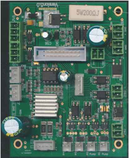
Switching power supply is to use the circuit to control the switching tube for high-speed on-off and...

What does a multi-layer PCB look like? High-end PCB board design process
18Jun
Caddy 0 Comments

What does a multi-layer PCB look like? High-end PCB board design process

Layout engineers think about it! No longer afraid of not painting!Think about purchasing want to cry...

PCB Lecture Hall: The difference between aluminum substrate and FR4 board
18Jun
Caddy 0 Comments

PCB Lecture Hall: The difference between aluminum substrate and FR4 board

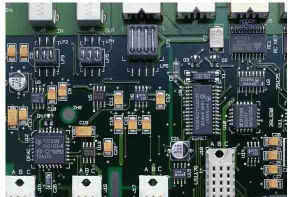
Electromagnetic shielding: In order to ensure the performance of the circuit, some components in ele...

High Speed PCB design Ten tips for PCB lamination design
18Jun
Caddy 0 Comments

High Speed PCB design Ten tips for PCB lamination design

The classic PCB laminated design is almost all even layers, rather than odd layers. Even layers of p...

The debugging procedure and method of PCBA machining
18Jun
Caddy 0 Comments

The debugging procedure and method of PCBA machining

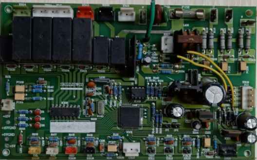
Firstly, the overcurrent protection current is preset, and then the voltage value of the regulated p...

PCB design layout constraints
18Jun
Caddy 0 Comments

PCB design layout constraints

The layout of the components should be convenient for signal flow, so that the signal is as consiste...

The whole process of PCB PCBA processing is introduced
18Jun
Caddy 0 Comments

The whole process of PCB PCBA processing is introduced

After welding parts to use the soldering iron and tin wire, welding will be maintained at a high tem...

What is the difference between aluminum substrate and FR4 plate?
18Jun
Caddy 0 Comments

What is the difference between aluminum substrate and FR4 plate?

In order to ensure the performance of the circuit, some components in the electronic product need to...

Reasons for internal shrinkage design of GND layer and power layer in multi-layer PCB design
18Jun
Caddy 0 Comments

Reasons for internal shrinkage design of GND layer and power layer in multi-layer PCB design

the power plane should be inside the PCB, and the upper and lower layers adjacent to him are 0V plan...

Just upload Gerber files, BOM files and design files, and the KINGFORD team will provide a complete quotation within 24h.