
Professional PCB manufacturing and assembly
Building 6, Zone 3, Yuekang Road,Bao'an District, Shenzhen, China
+86-13410863085Mon.-Sat.08:00-20:00

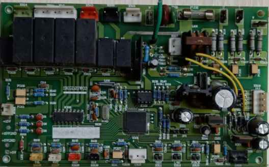
After PCBA processing is completed, it is necessary to debug the circuit board to verify whether its function meets the design requirements. This is a set of system engineering. Panel observation and resistance check.
First of all, we must roughly observe whether there are problems on the board, such as whether there are cracks, short circuit, open circuit and other phenomena. If necessary, check that the resistance between the power supply and the ground is large enough.
")
2. Install components Independent modules, in the absence of assurance that they work properly, it is best not to install all, but part by part, so that it is easy to determine the PCB fault range.
3. Check the output voltage of the power supply
In general, you can install the power supply part first, and then power on to detect whether the output voltage of the power supply is normal. When powering on, you can consider using an adjustable voltage regulated power supply with current limiting function.
4. Preset overcurrent protection current
Firstly, the overcurrent protection current is preset, and then the voltage value of the regulated power supply is gradually increased, and the input current, input voltage and output voltage are monitored. If there are no problems such as over-current protection during the up-regulation process, and the output voltage also reaches normal, it indicates that the power supply is normal.
5. Install other modules and test them
Gradually install other modules, each module installed, power on the test to avoid the design error or component installation error, resulting in overcurrent and burn components.
1.Maximum board: 310mm*410mm(SMT);
2. Maximum plate thickness: 3mm;
3. Minimum plate thickness: 0.5mm;
4. Minimum Chip parts: 0201 package 0.6mm*0.3mm or more parts;
5. Maximum mounting parts weight: 150g;
6. Maximum part height: 25mm;
7. Maximum part size: 150mm*150mm;
8. Minimum pin part spacing: 0.3mm;
9. Minimum ball parts (BGA) spacing: 0.3mm;
10. Minimum ball part (BGA) ball diameter: 0.3mm
11. Maximum part mounting accuracy (100QFP) : 25um@IPC;
12. Patch capacity: 3-4 million points/day.
kinhford Electronics Co., Ltd. specializes in providing integrated PCBA electronic manufacturing services, including upstream electronic component procurement to PCB production and processing, SMT patches, DIP plug-ins, PCBA testing, finished product assembly and other one-stop services.
The company gives full play to its competitive advantages in scale procurement and quality control, and has signed long-term cooperation agreements with many electronic component manufacturers at home and abroad and around the world to ensure the quality and stable supply of raw materials, and transfer the benefits to customers.


Just upload Gerber files, BOM files and design files, and the KINGFORD team will provide a complete quotation within 24h.