
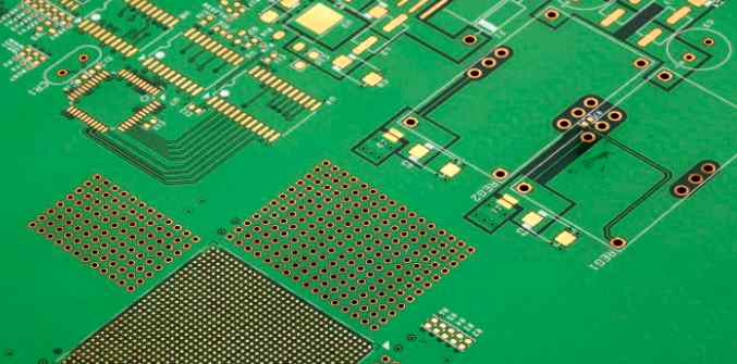
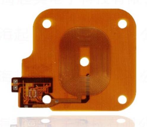
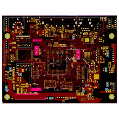
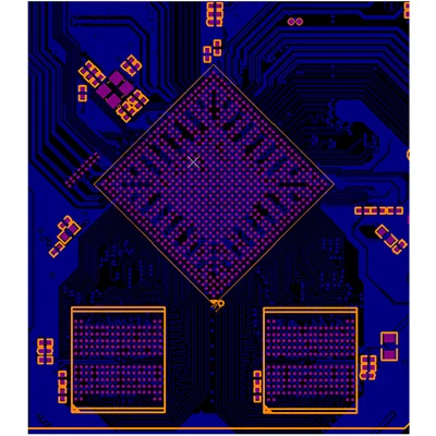
What are the main challenges of 5G communication to PCB process?
Live broadcast online
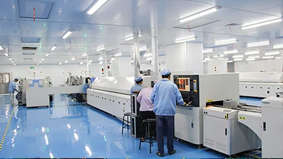


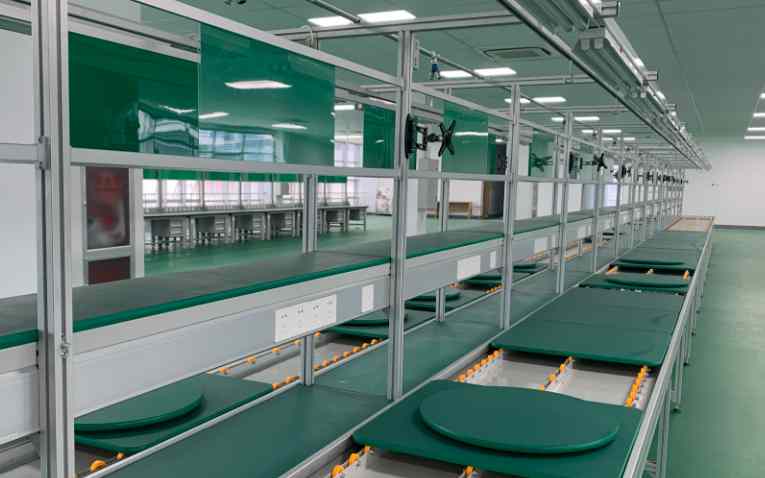
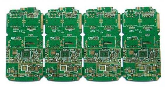
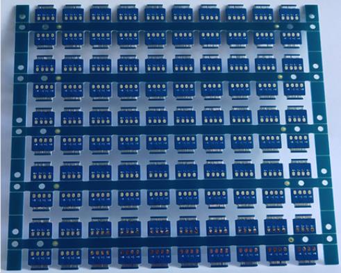
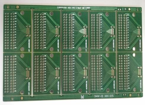
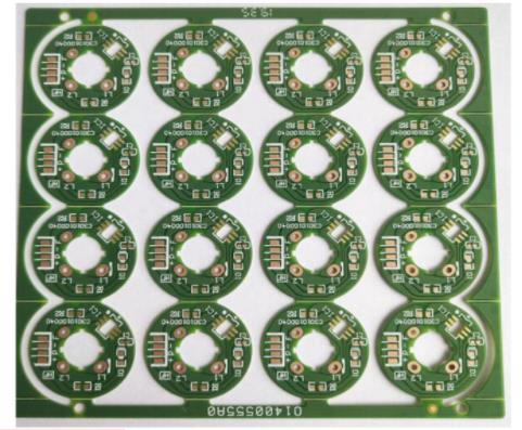
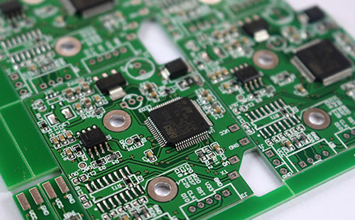
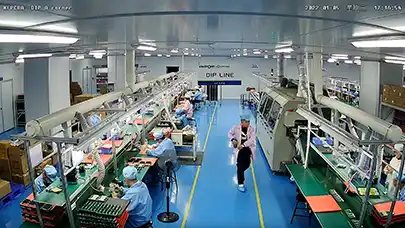

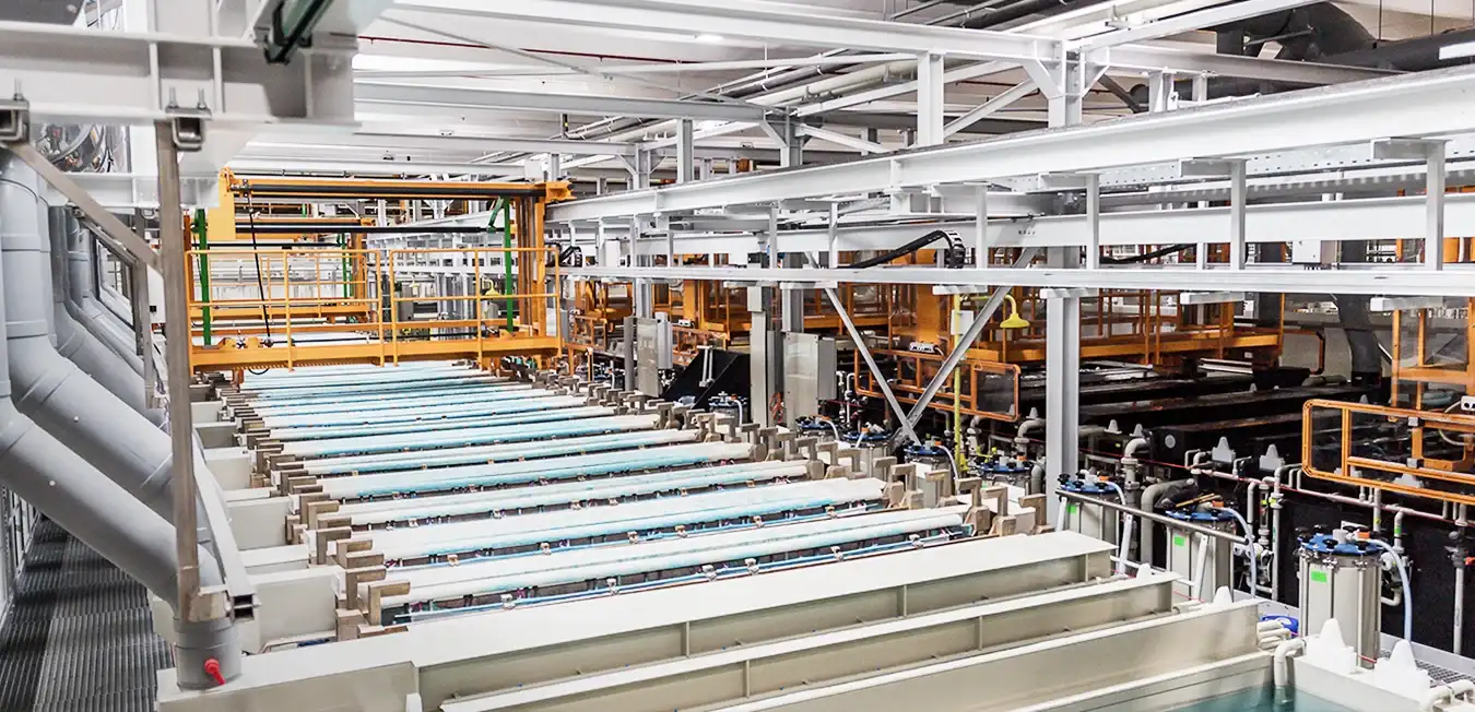
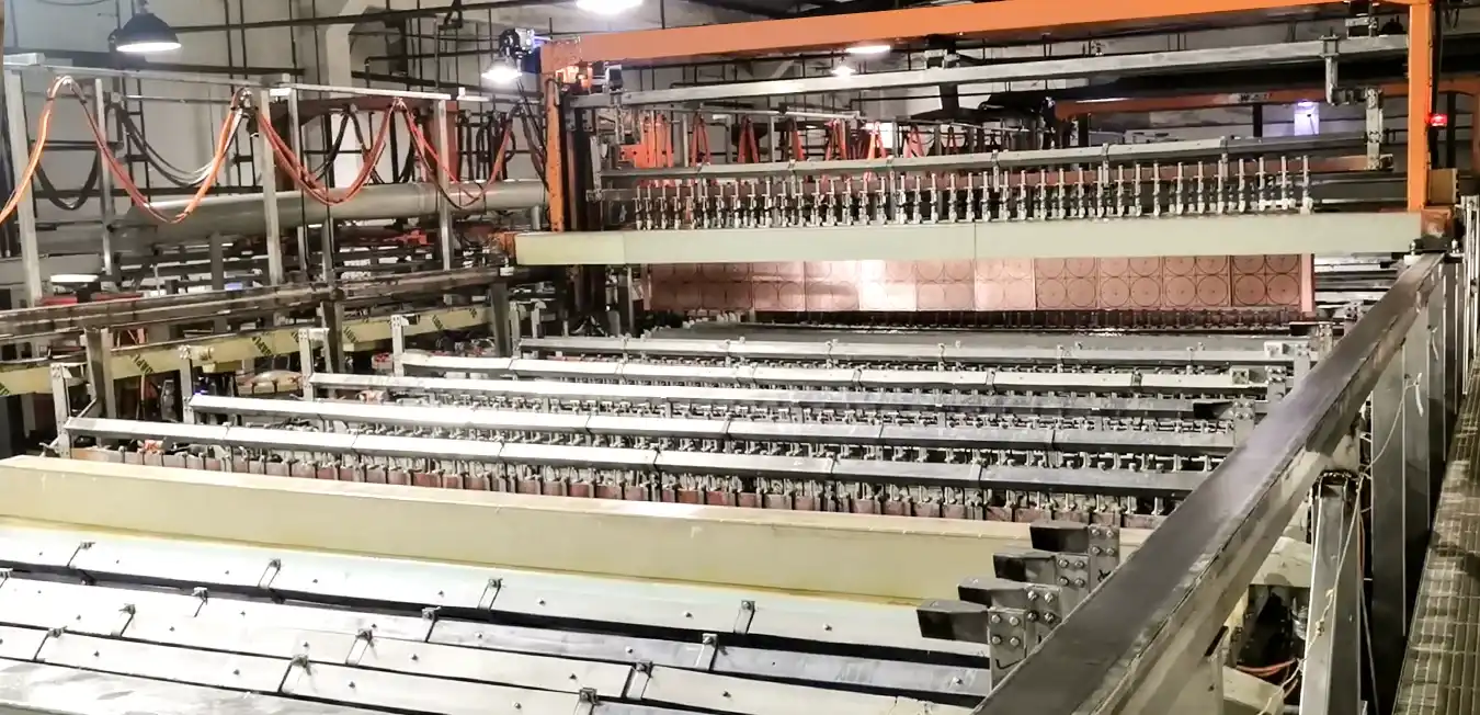
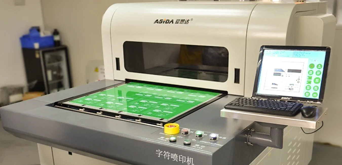
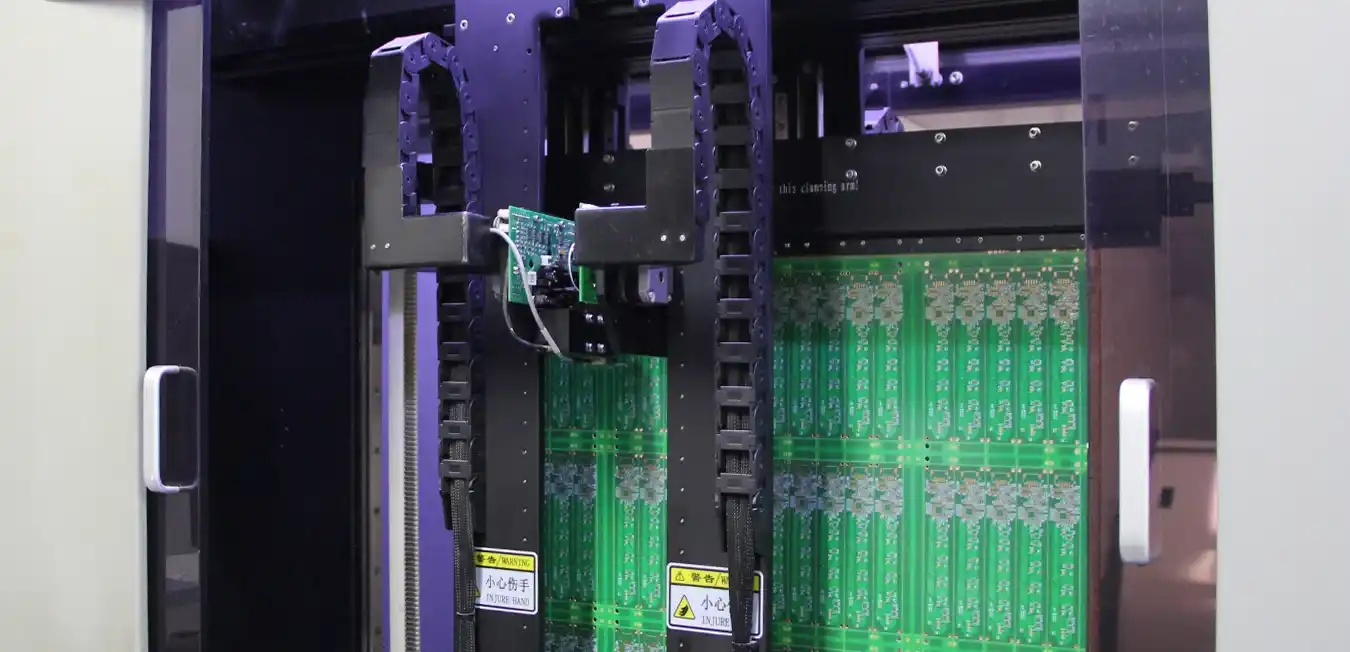
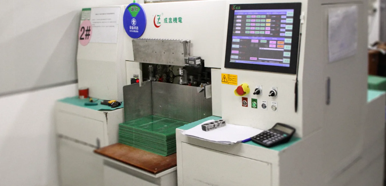
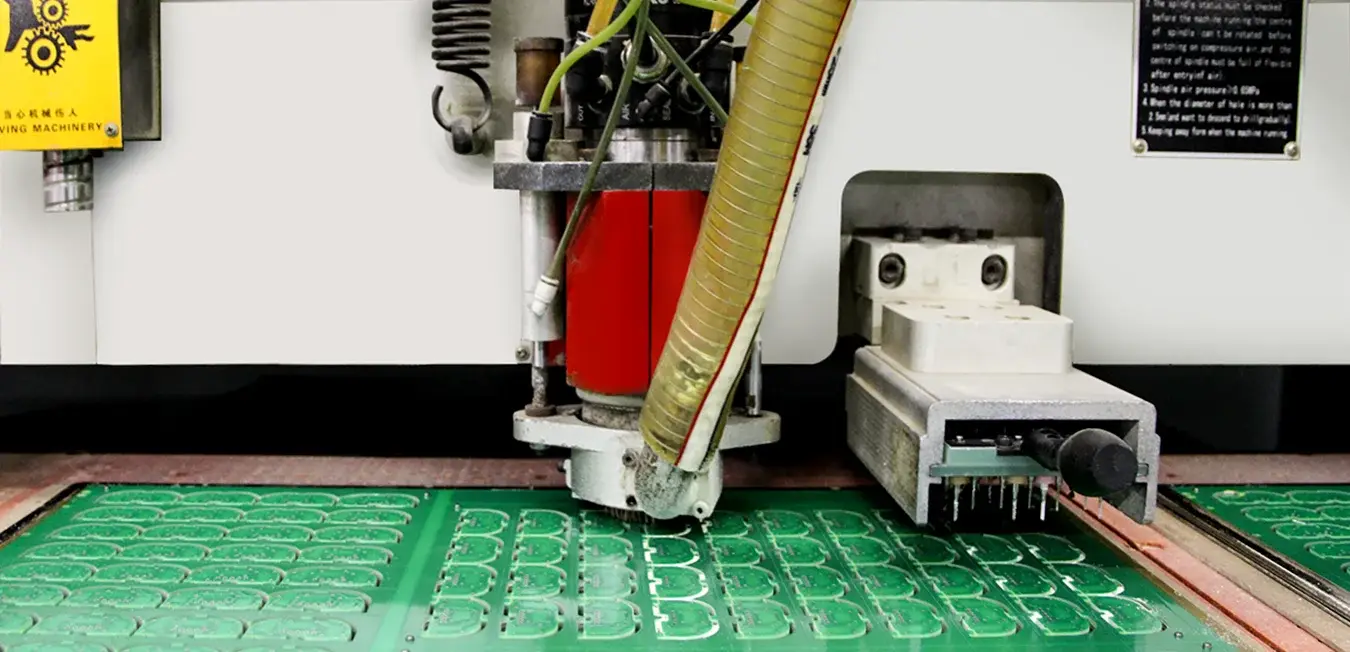
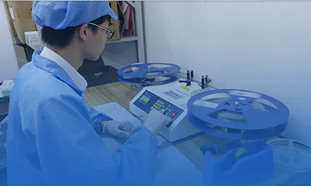
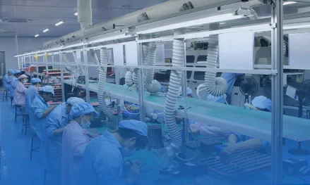
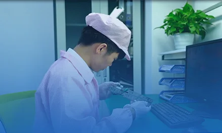
Kingford has its own 5000 square meters workshop, and is equipped with laser marking machine board, laser cutting machine,
CNC drilling machine, PCB laminating machine, PCB silk screen printing, PCB CNC machine tool, automatic PCB tester,
PCB two-dimensional inspection, PCB flying Needle tester and other equipment, is committed to building a first-class
production line, escorting the price of PCB quality.
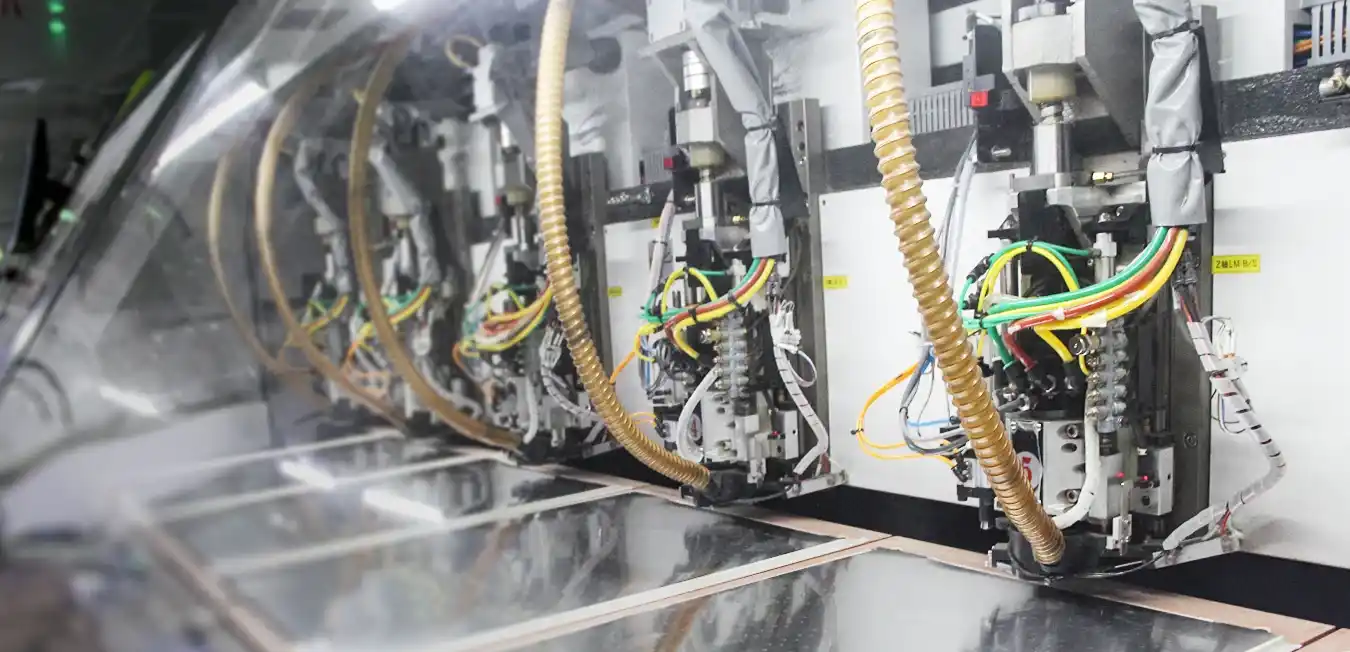
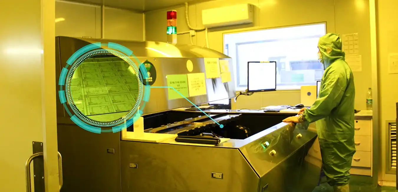
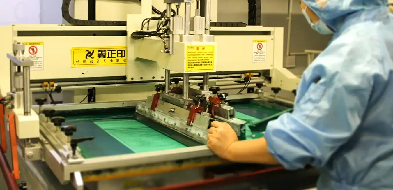
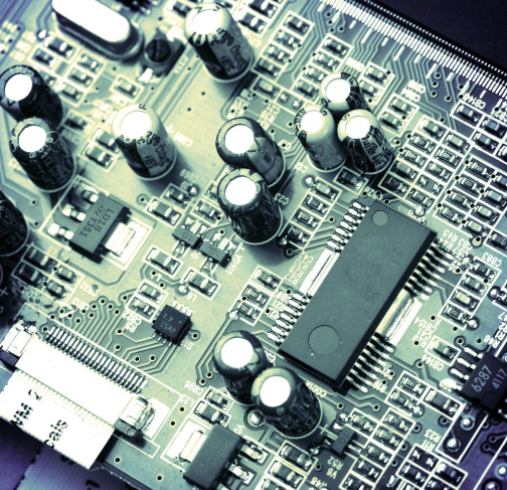
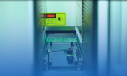
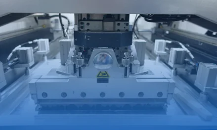
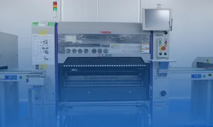
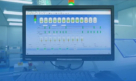
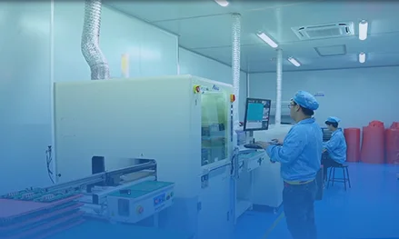
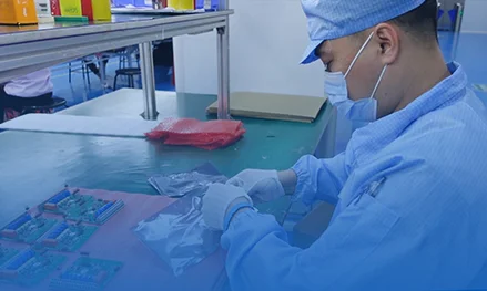
We have newly imported Yamaha high-end equipment, which can realize standardized production from solder paste printing,
SPI testing, reflow soldering and other links, which can improve production efficiency. Warehousing - Express" standardized process.
Point material storage
Loader
Solder Paste Printing
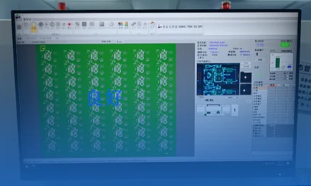
SPI
Surface mount
Nitrogen reflow soldering
First article inspection
DIP
QA detection
Three anti-coating
Package
