What are the matters needing attention and manufacturing process of PCB?
The production of Keyou circuit cannot be separated from your design. All engineers please design according to the detailed production process of conventional production.


The production of Keyou circuit cannot be separated from your design. All engineers please design according to the detailed production process of conventional production.
The plug technology meets the following requirements :1. Copper can be found in the through hole, but the plug cannot be used for resistance welding. 2. There must be tin lead in the through hole, with a certain thickness requirement (4 microns). Do not a
Purpose and precautions of reserved process edge in PCB design: Reserved process edge is the part added on both sides or four sides of PCB board to assist patch plug-in welding, which is mainly to assist production and does not belong to the PCB board. It

PCB design layer number to consider the following problems: 1, use,2, required signal type,3, through hole type,4, required signal layer density and number,5, required plane number,6, manufacturing cost,7, delivery time,
Analysis of the deformation causes of PCB board in the process of processing: 1. Incoming material of copper clad plate: 2. Pressing: 3. Welding resistance, character and other baking process: 4. Hot air solder leveling: 5. Storage
Single-side backwelding boards are rarely used now, because double-side backwelding can save space on the circuit board, which means it can make the production smaller.
In the process of PCB board copying, since the circuit board needs to be split, the integrated circuit and other components are removed to make BOM list, and the bare PCB board is scanned and copied.
In the actual study, it is found that PCB design mainly has four aspects of interference: power supply noise, transmission line interference, coupling and electromagnetic interference (EMI).
In the design of PCB electromagnetic compatibility, the main problem that needs attention is the interference problem of power supply and ground.
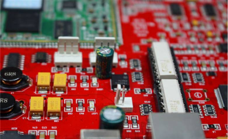
Double-sided PCB is a printed board with conductive graphics on both sides. It is usually made of epoxy glass cloth covered with copper foil board. It is mainly used in equipment with high performance requirements.
In the process of PCBA production, the selection of PCBA transtin is also very important. In the process of through hole plug-in, tin penetration is not good, which is easy to cause problems such as virtual welding, tin cracking and even falling parts.
The PCB processing process from the inner line pattern transfer of PCB substrate to the outer line pattern transfer by pressing several times will cause different growth and contraction of the warp and weft of the jointed board.


