
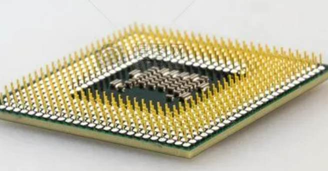
Professional PCB manufacturing and assembly
Building 6, Zone 3, Yuekang Road,Bao'an District, Shenzhen, China
+86-13410863085Mon.-Sat.08:00-20:00

First-class production comes from first-class design. The production of Keyou circuit cannot be separated from your design. All engineers please design according to the detailed production process of conventional production.
Details of relevant design parameters:
I. via hole (commonly known as conductive hole)
1. Minimum aperture :0.3mm(12mil)
2. The minimum hole (VIA) aperture is not less than 0.3mm(12mil), the single side of the pad can not be less than 6mil(0.153mm), the best greater than 8mil(0.2mm) is not limited to this point is very important, the design must be considered
3. Through hole (VIA) hole to hole spacing (hole edge to hole edge) should not be less than :6mil preferably greater than 8mil This point is very important, design must be considered
4. Spacing between pad and contour line 0.508mm(20mil)

Ii. Circuit
1. Minimum line distance: 6mil (0.153mm). Minimum line distance, that is, line to line, line to pad distance is not less than 6mil from the production point of view, the bigger the better, generally in 10mil, of course, under the condition of design conditions, the bigger the better this point is very important, the design must consider.
2. Minimum line width: 6mil (0.153mm). That is to say, if the line width is less than 6mil, the production will not be possible (the minimum line width of the inner layer of multilayer board is 8MIL). If the design conditions permit, the larger the design, the better, the larger the line width, the better our Huaqiang PCB factory production, the higher the yield, the general design routine around 10mil is very important, the design must be considered.
3. Distance between line and contour line 0.508mm(20mil)
Three, PAD pad pad (commonly known as the plug-in hole (PTH))
1 plug-in hole (PTH) welding disc outer ring side can not be less than 0.2mm(8mil) of course, the bigger the better this point is very important, the design must be considered
2 plug-in hole (PTH) hole to hole spacing (hole edge to hole edge) can not be less than: 0.3mm of course, the bigger the better this point is very important, the design must be considered
3. The size of the plug-in hole depends on your components, but it must be larger than the pin of your components. It is recommended that the pin of the components should be larger than 0.2mm at least, that is to say, the pin of the components of 0.6 should be designed as 0.8 at least, in case it is difficult to insert due to machining tolerance.
4. Spacing between pad and contour line 0.508mm(20mil)
Four, anti-welding: plug-in hole window, SMD window side shall not be less than 0.1mm(4mil)
Five, character (character design, directly affect the production, whether the character is clear to the character design is very relevant)
1. Character width can not be less than 0.153mm(6mil), the height of the word can not be less than 0.811mm(32mil), the ratio of width to height of the best 5 relationship is that is to say, the word width of 0.2mm word height of 1mm, to push the class
Six, non-metallic slot: the minimum spacing of slot is not less than 1.6mm, otherwise it will greatly increase the difficulty of milling edge
Seven, patchwork
1. Patchwork without gap patchwork, and with gap patchwork, with gap patchwork gap should not be less than 1.6(plate thickness 1.6)mm, otherwise it will greatly increase the difficulty of milling edge, the size of the patchwork board depending on the equipment is not the same, No gap patchwork gap about 0.5mm process edge can not be less than 5mm. (Keyou circuit focus on PCB circuit board rapid proofing and batch! (FR-4 glass fiber board/copper substrate/aluminum substrate) business advisory hotline: 13723490391 bell S)
Related matters needing attention
First, original documents on PADS design
1. Select the Through attribute for dual-panel PADS, instead of Partial buried holes. Drilling files cannot be generated and drilling holes will be missed.
2. Do not add slots in PADS together with components, because GERBER cannot be generated normally. In order to avoid leaking slots, please add slots in DrillDrawing.
3. The PADS are paved in copper mode, and the manufacturer uses Hatch mode for copper paving. After the customer's original documents are moved, they should be paved with copper again for preservation (using Flood) to avoid short circuit.
Two, about PROTEL99SE and DXP design documents
1. The manufacturer Solder depends on the Solder mask layer. If the Paste layer needs to be made and GERBER cannot be generated in the solder window with more layers, please move to the solder mask.
2. Do not lock the contour line in the Protel99SE. GERBER cannot be generated normally.
3. Do not select KEEPOUT option in the DXP file; otherwise, the appearance line and other components will be kept blank, and GERBER cannot be generated.
4. Please pay attention to the positive and negative design of these two documents. In principle, the top layer is positive, and the bottom layer is designed to be negative. Single plate in particular, do not mirror at will! It might be the other way around.
Three. Other points to note
1. Shapes (such as plate frame, slot, V-CUT) must be placed on KEEPOUT layer or mechanical layer, not on other layers, such as screen printing layer and line layer. All slots or holes that need mechanical molding should be placed in one layer as far as possible to avoid leaking slots or holes.
2. If the shape of the mechanical layer and the KEEPOUT layer is inconsistent, please make special instructions. In addition, the shape should be given to the effective shape. If metal holes need to be processed, please make special remarks.
3. With three kinds of software design, please pay special attention to whether the key position needs to expose copper.
4. If you want to do the most secure way to metalize the slot is to put together a number of pads, this practice must not be wrong
5. Please make special remarks on whether bevel chamfering is required for the order of goldfinger plate.
6. Please check whether there are fewer layers in the GERBER file. Generally, the manufacturer will make the GERBER file directly.
7. Under normal circumstances, gerber is named in the following ways:
Component surface circuit: gtl component surface welding: gts
Component surface character: gto welding surface line: gbl
Welding face Welding face: gbs Welding face character: gbo
Appearance: gko Layout :gdd
Drilling: drll
How can PCBA avoid PCB board warping?
Mar 03,2023


Just upload Gerber files, BOM files and design files, and the KINGFORD team will provide a complete quotation within 24h.