
Professional PCB manufacturing and assembly
Building 6, Zone 3, Yuekang Road,Bao'an District, Shenzhen, China
+86-13410863085Mon.-Sat.08:00-20:00

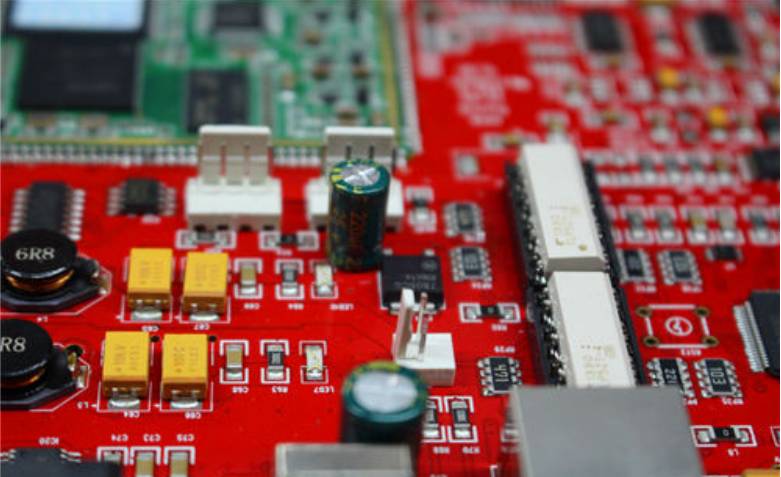
At present, the mainstream circuit board assembly technology in SMT industry should be "Reflow", and of course there are other circuit board welding methods, which can be divided into single board reflow and double board reflow. Single-side reflow is rarely used now, because double-side reflow can save space on the circuit board. That is to say, it can make the production smaller, so most of the boards on the market belong to the double-sided back welding process.
Because of the "double-sided backwelding process" need to do two backwelding relationship, so there will be some restrictions on the process, the most common problem is that the board to the second backwelding furnace, the first side of the above parts will fall because of gravity, especially the board flow to the furnace backwelding area high temperature, this paper will explain the double-sided backwelding process parts placement precautions:
1. Which SMD parts should be placed on the first side of the back welding furnace?
Generally speaking, small parts are recommended to be placed in the first side of the backwelding furnace, because the deformation of PCB will be relatively small when the first side of the backwelding furnace, and the precision of solder paste printing will be relatively high, so it is better to put small parts together.
Second, smaller parts do not risk falling off the second time through the furnace. Because the first side of the parts in the second side will be placed on the bottom of the printed circuit board directly down, when the board into the weld area of high temperature will not fall down from the board because of weight.
Third, the first side of the board parts must have two back welding furnace, so the temperature must be able to withstand two back welding temperature, general resistance capacitance is usually required to at least three times back welding high temperature, this is in order to meet some of the board may be due to the maintenance of the relationship, need to go back to a welding furnace and do the requirements.
2. Which SMD parts should be placed on the second side of the back welding furnace?
Large or heavy components should be placed on the second side of the furnace to avoid the risk of parts falling back into the furnace during the furnace.
LGA, BGA parts should be placed on the second side of the furnace as far as possible, so as to avoid the unnecessary risk of remelting tin during the second furnace, so as to reduce the chance of empty/false welding. If the BGA parts with thin interstitials and small is not excluded, it is recommended to place in the first side of the back welding furnace.
BGA placed on the first or second side of the furnace has been very controversial, placed on the second side although can avoid the risk of re-melting tin, but usually the second side of the back welding furnace PCB deformation is more serious, but will affect the quality of eating tin, so the working bear will not exclude the thin foot of the BGA can be considered on the first side. But on the other hand, if PCB deformation is serious, as long as the fine parts, placing the patch on the second side must be a big problem, because the solder paste printing position and solder paste amount will become inaccurate, so the focus should be on how to avoid the deformation of the circuit board, rather than considering the BGA on the first side because of deformation, right? Parts that cannot withstand too many high temperatures should be placed in the second side of the back welding furnace. This is to prevent the parts from being damaged by too much heat.
PIH/PIP parts should also be placed on the second side of the furnace. Unless the length of the welding foot does not exceed the plate thickness, the foot extending out of the PCB surface will interfere with the second side of the steel plate, which will make the second side of the solder paste printed steel plate cannot be attached to the PCB, resulting in abnormal solder paste printing.
Some components will have the use of soldering operations inside the situation, such as LED light cable connectors, we must pay attention to the temperature resistance of this part can be twice back welding furnace, if not placed in the second side of the piece.
Just the parts placed on the second side of the piece patch back welding furnace, it means that the circuit board has been a high-temperature baptism of the welding furnace, at this time the circuit board has some warping and deformation, that is to say, the printing amount of solder paste and printing position will become more difficult to control, so it is easy to cause air welding or short circuit and other problems, so placed on the second side of the furnace parts, It is recommended that 0201 and fine pitch parts should not be placed as far as possible. BGA should also try to choose tin balls with larger diameters.
In addition, in the mass production of electronic parts to be welded and assembled on the circuit board, in fact, there are many technological methods, but each process is actually in the PCB design has been decided at the beginning, because the placement of the parts on the circuit board will directly affect the assembly of welding sequence and quality, and wiring will indirectly affect.
At present, the welding process of circuit board can be roughly divided into full plate welding and partial welding, and full plate welding can be roughly divided into Reflow Soldering and Wave Soldering. The partial welding of circuit board includes Carrier Wave Soldering, Selective Soldering, non-contact Laser soldering, etc.


Just upload Gerber files, BOM files and design files, and the KINGFORD team will provide a complete quotation within 24h.