
Professional PCB manufacturing and assembly
Building 6, Zone 3, Yuekang Road,Bao'an District, Shenzhen, China
+86-13410863085Mon.-Sat.08:00-20:00


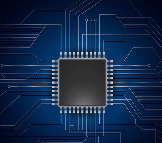
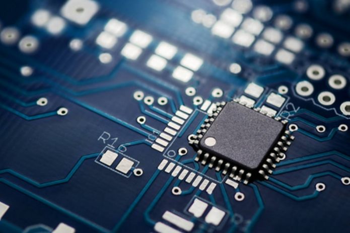
The problem of anti-interference is a very important link in modern circuit design, which directly reflects the performance and reliability of the whole system. For PCB engineer, anti-interference design is the key and difficult point that we must master.
The presence of interference in PCB board
In the actual study, it is found that PCB design mainly has four aspects of interference: power supply noise, transmission line interference, coupling and electromagnetic interference (EMI).

1. Power supply noise
In the high frequency circuit, the noise of the power supply has an obvious influence on the high frequency signal. Therefore, the first requirement is that the power supply be low noise. Clean land is just as important here as clean power.
2. Transmission line
Only two types of transmission lines are possible in PCBS: strip and microwave lines. The biggest problem of transmission line is reflection, reflection will cause a lot of problems, for example, the load signal will be the superposition of the original signal and the echo signal, increase the difficulty of signal analysis; Reflection will cause return loss (return loss), and its effect on the signal is as serious as that of additive noise interference.
3. Coupling
The interference signal generated by the interference source can cause electromagnetic interference to the electronic control system through a certain coupling channel. The coupling mode of interference is nothing more than through wire, space, common line, etc. acting on the electronic control system. The analysis mainly includes the following types: direct coupling, common impedance coupling, capacitance coupling, electromagnetic induction coupling, radiation coupling, etc.
4. Electromagnetic Interference (EMI)
Electromagnetic interference There are two types of EMI: conduction interference and radiation interference. Conducted interference refers to the coupling (interference) of signals from one electrical network to another electrical network through a conducting medium. Radiation interference refers to the coupling (jamming) of the interference source to another electrical network through space. In the design of high-speed PCB and system, high frequency signal lines, pins of integrated circuits, various connectors and so on May become radiation interference sources with antenna characteristics, which can emit electromagnetic waves and affect the normal work of other systems or other subsystems within the system.
PCB and circuit anti-jamming measures
The anti-interference design of printed circuit board has a close relationship with the specific circuit, next, we only on the PCB anti-interference design of several common measures to do some explanation.
1. Power cord design
According to the size of the printed circuit board current, try to thicken the width of the power line to reduce the loop resistance. At the same time, the direction of the power cord and ground wire is consistent with the direction of data transmission, which helps to enhance the anti-noise capability.
2. Ground wire design
Digital and analog separately. If the circuit board contains both logical and linear circuits, keep them as separate as possible. Low frequency circuit should be as far as possible to use a single point of parallel grounding, the actual wiring difficulties can be partially connected after the parallel grounding. High frequency circuit should adopt the multi-point series grounding, the ground should be short and thick, high frequency components around as far as possible with a large area of grid foil.
The ground cable should be as thick as possible. If the grounding wire is very thin, the grounding potential changes with the change of current, so that the noise resistance performance is reduced. The ground wire should therefore be thickened so that it can pass through three times the allowable current on the printed board. If possible, the ground cable should be at least 2 mm to 3mm.
The ground wire forms a closed loop. For printed boards composed only of digital circuits, the ground circuit is arranged into a group loop, which can improve the noise resistance.
3. Configuration of decoupling capacitor
One of the common practices of PCB design is to configure appropriate decoupling capacitors in various key parts of the printed board.
The general configuration principles of decoupling capacitors are:
① The power input end is connected to the 10 ~100uf electrolytic capacitor. If possible, 100uF + is preferable.
② In principle, each integrated circuit chip should be arranged with a 0.01pF ceramic capacitor. If the gap of the printed board is not enough, a capacitor of 1-10pF can be arranged every 4~8 chips.
(3) For devices with weak noise resistance and large power supply changes when the device is turned off, such as RAM and ROM memory devices, the decoupling capacitor should be directly connected between the power cord and the ground wire of the chip.
④ The capacitor lead should not be too long, especially the high-frequency bypass capacitor should not have a lead.
4. Methods of eliminating electromagnetic interference in PCB design
① Reduce the loop: Each loop is equivalent to an antenna, so we need to minimize the number of loops, the area of loops and the antenna effect of loops. Ensure that the signal has only one loop path at any two points, avoid artificial loops, and try to use the power layer.
② Filtering: In the power line and in the signal line can be taken to reduce EMI filtering, there are three methods: decoupling capacitor, EMI filter, magnetic element.
③ Shield.
④ Reduce the speed of high-frequency devices as far as possible.
⑤ Increasing the dielectric constant of PCB board can prevent the high frequency parts such as the transmission line near the board from radiating outward; Increasing the thickness of PCB board and minimizing the thickness of microstrip line can prevent electromagnetic line spillover and also prevent radiation.


Just upload Gerber files, BOM files and design files, and the KINGFORD team will provide a complete quotation within 24h.