
Professional PCB manufacturing and assembly
Building 6, Zone 3, Yuekang Road,Bao'an District, Shenzhen, China
+86-13410863085Mon.-Sat.08:00-20:00

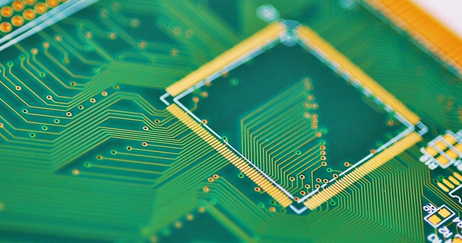
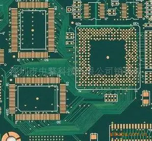
PCB wiring rules of thumb
Today, there are still some rules of thumb for PCB wiring that were common 20 years ago. Are they still widely observed and applied? The exact answer is "maybe". Some rules on obeying/avoiding wiring in PCB design forums enable PCB designers to either observe or ignore these rules where they may not apply. In some cases, this may not necessarily result in a circuit board design failure. As some experienced PCB designers said, the circuit board can work normally just by chance.
The discussion on PCB design rules of thumb does not mean that they are correct or wrong. The problem is that these discussions are often lack of application relevance, which also makes the discussion duration of rules mentioned in the forum. This article hopes to make clear the scenarios that these rules adapt to, when different rules are applied, and when to avoid accurate interpretation.

Common rules of thumb in PCB wiring
1. Vertical wiring
The rule of vertical wiring is that the leads of adjacent signal layers need to be perpendicular to each other to reduce crosstalk caused by mutual inductance. In high frequency signals, crosstalk generated by capacitive coupling is the main component, which generates current spikes between vertical leads.
When the signal changes over time or the frequency is low (less than several GHz), the coupling capacitance interference of the vertical wiring devices of adjacent signal layers is small. In the radio frequency (RF) frequency band (dozens of GHz), the interweaving of leads produces hole resonance, and the conductor structure not surrounded by the ground wire will produce electromagnetic resonance at some special frequency points. At this time, even if the leads are vertical, strong crosstalk will be caused between them.
In order to eliminate interference at all frequency points, a simple and effective method is to use multilayer boards and isolation layers between signal layers. It is especially important in the application of modern high-speed signal change. When you are not sure about the coupling strength between orthogonal lines, you need to use the basic crosstalk simulation software to check the vertical leads to see whether the crosstalk between them is within the noise tolerance range. At this point, you need to plan the signal return path, which is a major problem in vertical cabling.
2. Heat dissipation via
This is a classic "observe/avoid" rule, which often causes controversy. Some PCB designers say that they never use heat dissipation vias and have never encountered problems with welding and assembly. Another group insisted on preventing heat dissipation vias from being used when each plane is connected. Who are they right?
Their views are applicable to different occasions. If you weld the circuit board manually, you need to increase the temperature of the soldering head to compensate for the soldering problem caused by the heat dissipation of the copper layer caused by the soldering via. However, if wave soldering is used, it is necessary to use anti heat dissipation vias to prevent devices from loosening, cold welding, erecting, etc., so I suggest you stick to the anti heat dissipation vias design.
3. Right angle wiring
This PCB wiring rule is perhaps the most beloved and hated. Today, I still see many PCB designers insist that at any time the wiring can not turn a right angle for various reasons. For example, they say that it is difficult for electrons to turn right angles when moving in the lead, but they do not think that all vias on the circuit board are perpendicular to the lead. There are also some reasons that are more reliable. For example, the lead length can be reduced through 45 ° corners, and all right angle turn wiring needs chamfering. It is also said that the right angle turn will produce acid etching traps in the acid etching solution of the circuit board, which is not the problem in the alkaline etching solution widely used nowadays.
Unless your circuit board works in the high frequency (involving millimeter wave radar/5G communication) circuit above 50GHz, you don't need to worry about the lead turning right angle. In fact, when wiring the circuit board, you can use any angle you like to lay the leads. If you use PCB design software with built-in electromagnetic field solving function, it will make your wiring easier.
4. "3W" rule
That is, three wiring rules of thumb. The first version of the "3W rule" says that the spacing between two adjacent leads should be no less than three times the lead width, so as to reduce the magnetic flux coupling between leads and thus reduce the electromagnetic interference between leads.
This rule may forget that the electromagnetic coupling between leads is proportional to the overlapping area of lead circuit, not the distance between leads; Therefore, the overlap area of the lead circuit is reduced, and the lead spacing is not limited by the 3W rule. Just like the previous vertical wiring, the basic electromagnetic interference simulation can check the impact of different wiring spacing.
Another version of the "3W" rule refers to that when using zigzag wiring for lead length matching, the zigzag width needs to be greater than or equal to three times the lead width, which can minimize the discontinuity of lead impedance.
5. "20H" rule
This rule defines the overlapping distance between the ground wire layer and the power supply layer in a PCB. In modern PCB design, the power supply needs to be laid near the ground wire to ensure that there is sufficient interlayer capacitance between them, thus reducing power fluctuations on high-speed circuit boards.
But the actual measurement results will find that the results are very complex. Some time result standard names can reduce electromagnetic radiation by following the 20H rule at 300MHz. However, there will be high-frequency resonance between the ground wire and the power supply layer. Their structures are similar to waveguides, which will aggravate the high-frequency interference between lines.
So in practical application, if your circuit frequency is within GHz, you can follow the 20H rule, otherwise, the 20H rule may bring worse results


Just upload Gerber files, BOM files and design files, and the KINGFORD team will provide a complete quotation within 24h.