
Professional PCB manufacturing and assembly
Building 6, Zone 3, Yuekang Road,Bao'an District, Shenzhen, China
+86-13410863085Mon.-Sat.08:00-20:00


The simple truth of board design is that it must fit its intended application, not the other way around. Therefore, as a PCB designer, you will find that there are many different PCB size and shape requirements. Here are some ideas for great ways to use these different board dimensions.
Understand the size and shape requirements of the PCB before starting the layout
Given the annoyance of aggressive scheduling and design delays, it is understandable why some PCB layout designers would have their eyes open to start their board design. The problem, of course, is that they may be missing key design information, especially when it comes to size or profile size or board profile. Medium-sized design changes have become a reality when it comes to PCB layouts. One thing you need to do is deepen the impact of future changes without complete information from the start. Without good board profile data to work with upfront, you may face the possibility of having to do a lot of redesign later.
To avoid such problems, make sure you understand the size and shape requirements of your design before you begin layout. This includes not only the X and Y dimensions of the board, but also the height limits. This will require working closely with your entire design team to capture the information you need. And don't hesitate to ask as many questions as you can. You don't want to later suffer from having to replace many circuits in your design because you didn't realize that mounting holes would appear where the main processor would be placed.
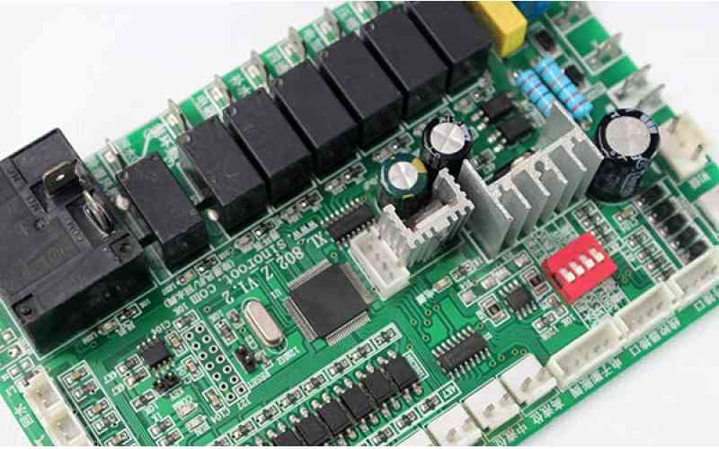
Now that you have the board data you need, you can use several different options to create the board outline.
In the past, PCB design tools have been more of a hindrance than a help in drafting objects such as board Outlines. Fortunately, these tools have evolved over the years, and users now have several options to create board Outlines.
You can draw a layout tool utility that allows designers to manually outline their boards. These tools will not only create the main Outlines for you, but will also add other Outlines for layout and wiring constraints. In addition, you can use the drawing function in the tool to manipulate contours and create arcs or other graphic features to finalize the size and shape you want.

Many design tools will also provide you with creation wizards that will automatically draft the board outline. The wizard not only contains tools to create the board outline, but also builds the board layer stack and sets the basic wiring width and spacing size. Such a wizard can save you a lot of time and effort in creating the board outline.
In addition to these drawing tools, modern PCB design CAD systems often provide you with other useful utilities to work with board Outlines. A very important feature when dealing with complex circuit board shapes is the ability to import mechanical CAD data into a PCB database. The data is available in a variety of different formats, including DXF, IDF, IDX and IPC-2581.
Your PCB design CAD system will read these formats and create the board outline accordingly. You can even save these Outlines as templates to use again and again in new designs. The key, of course, is to use a CAD system that supports all these different functions.
The importance of a complete design tool system
A good PCB design CAD system will not only be able to support different import formats and provide you with a large number of drawing tools, but will also provide many other benefits. One of the most useful features is the ability to display both the PCB layout and the mechanical design in the layout tool. This enables designers to see how their layouts work in the overall system design. With the 3D capabilities of the layout tool, designers can interactively handle their component placement in real time and correct all clearance errors in the design's mechanical features.
PCB board differential wiring operation skills
The popularity of high-speed serial bus makes more and more differential signals on PCB board. Then, how to differential wiring PCB board?
The impedance requirements of different kinds of difference lines are different. According to the design requirements, the difference impedance and the corresponding line width spacing are calculated through the impedance calculation software, and set to the constraint manager. The difference lines are coupled to each other to reduce common-mode interference. If conditions permit, they are routed as parallel as possible. There should be no holes or other signals between the two lines. In order to reduce the loss, a ground pass hole can be added near the layer-changing hole during the layer-changing of high-speed difference line.
Differential wiring operation skills:
1. Activate the wiring instruction, select Route→connect command, and then select the defined difference signal line. At this time, the defined difference signal line will be pulled out at the same time.
2. Single-wire mode is supported. When single-wire mode is required for local wiring, right-click the mouse button under the routing command and choose from the shortcut menu
Single Trace Mode Command mode.
3. When laying out differential wiring in small Spaces, you can switch to Neck Mode. In the same way, click the right mouse button in the wiring instruction state and select Neck Mode command from the shortcut menu.
4, according to the wiring needs to choose the appropriate differential hole mode. Click the right mouse button in the routing instruction state, and select the Via Pattern command from the shortcut menu.
Crosstalk in PCB design
Feb 10,2023


Just upload Gerber files, BOM files and design files, and the KINGFORD team will provide a complete quotation within 24h.