
Professional PCB manufacturing and assembly
Building 6, Zone 3, Yuekang Road,Bao'an District, Shenzhen, China
+86-13410863085Mon.-Sat.08:00-20:00

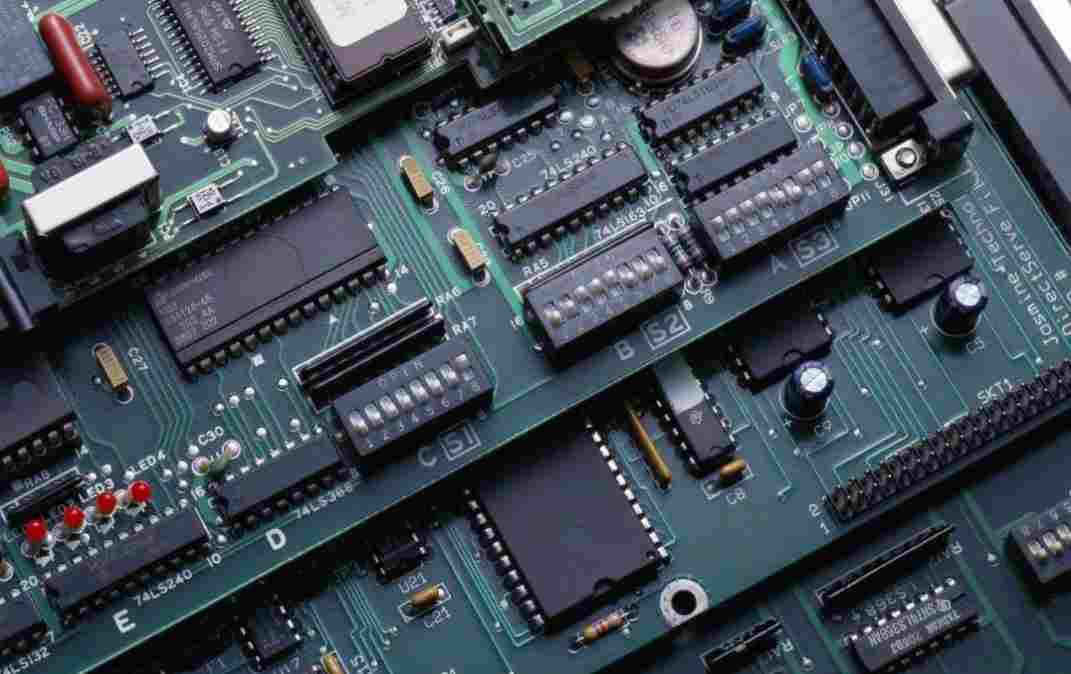
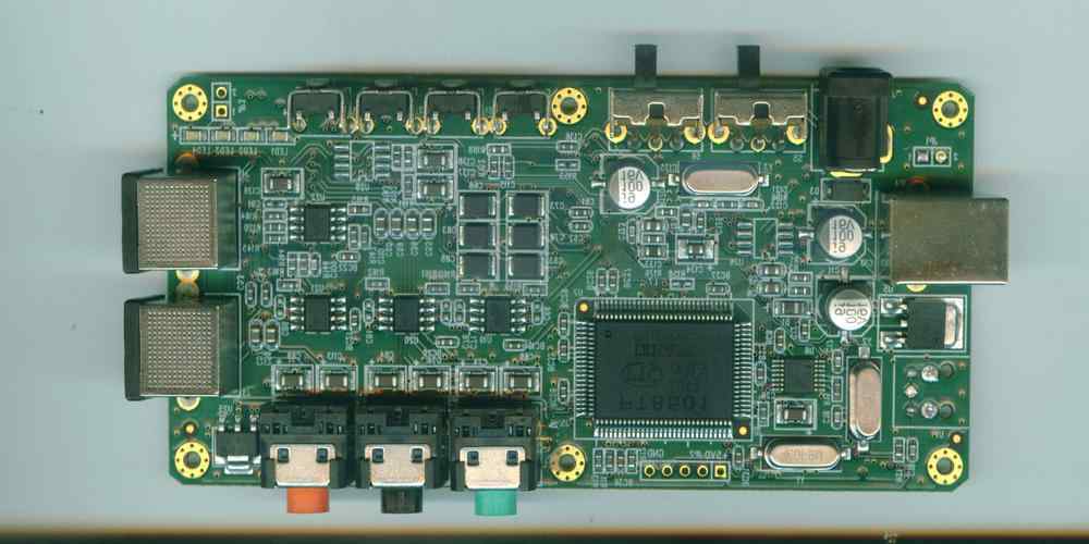
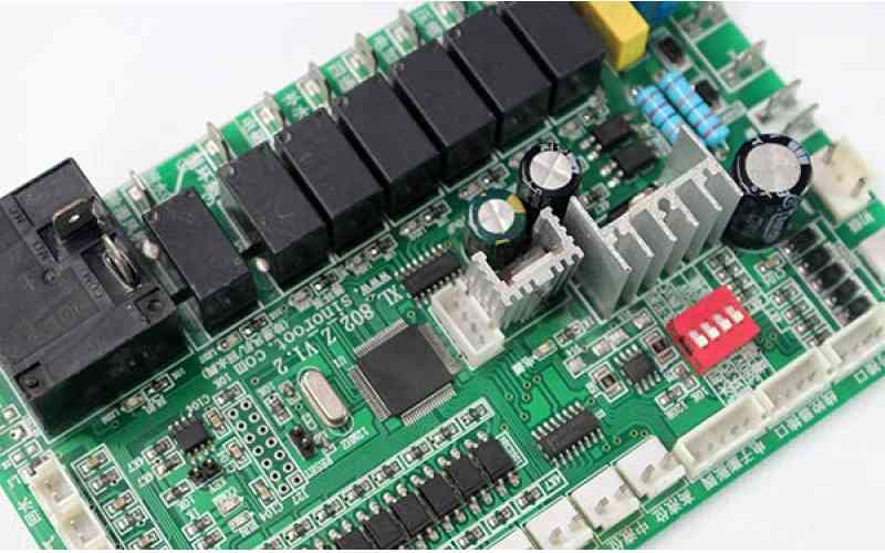
HDI board is one of the most precise PCB board, and its process is also more complex. The core steps include the formation of high precision printed circuit, the processing of micro through hole, the plating of surface and hole. Next, let's look at these core steps in HDI PCB platemaking.
1. Hyperfine circuit processing
With the development of science and technology, some high-tech equipment is more and more miniaturized and refined, so the HDI board used by it is also more and more high requirements.
In some devices, HDI circuit boards have grown from 0.13mm (5mil) to 0.075mm (3mil) in line width/line distance, and have become the mainstream standard.
The increasing line width/line distance requirement brings the most direct challenge to the graphic imaging in PCB fabrication process. So how do the copper wires on these precision plates form?
Current fine circuit formation processes include laser imaging (pattern transfer) and pattern etching forming.
Laser direct imaging (LDI) technology is used to obtain fine circuit graphics directly from laser scanning on the surface of copper coated with photoresist. Laser imaging technology greatly simplifies the process flow and has become the mainstream technology of HDI PCB plate-making.
Now used more and more is the half addition method (SAP) and improved half addition method (mSAP), that is, the pattern etching method. The technology can also realize the wire width of 5um conductive circuit.
2. Microporous processing
The important feature of the HDI circuit board is that it has a micro through hole (aperture ≤0.10mm), and these holes are buried blind hole structure.
At present, the buried blind holes on the HDI board are mainly processed by laser, but there are also CNC drilling.
Compared with laser drilling, mechanical drilling also has its own advantages. When laser processing epoxy glass cloth medium layer through hole, due to the difference in ablation rate between glass fiber and the surrounding resin, the quality of the hole will be slightly poor, and the residual glass fiber on the hole wall will affect the reliability of the through hole. Therefore, the superiority of mechanical drilling is reflected at this time. In order to improve the reliability and drilling efficiency of PCB board, laser drilling and mechanical drilling technology has been steadily improved.
3. Electroplating and surface treatment
How to improve the plating uniformity and plating deep hole ability in PCB manufacturing, improve the reliability of the circuit board. This depends on the continuous improvement of electroplating process, from the ratio of electroplating solution, equipment deployment, operating procedures and other aspects.
High frequency sound waves can accelerate the ability to etch; Permanganic acid solution can enhance the decontamination ability of the workpiece. The high frequency acoustic wave will stir in the plating tank and add a certain proportion of potassium permanganate plating solution. This helps the plating solution flow evenly into the hole. Thus, the deposition capacity and uniformity of electroplating copper can be improved.
At present, the blind hole of copper plating filling hole is relatively mature, can be different aperture of through hole filling copper. The two-step copper plating can be applied to the through hole with different aperture and height-thick-diameter ratio, and has a strong copper filling ability, which can minimize the thickness of the surface copper layer.
There are a variety of options for the final surface coating of PCB board. Electroless nickel/gold plating (ENIG) and electroless nickel/palladium/gold plating (ENEPIG) are commonly used in high-end PCBS.
ENIG and ENEPIG both have the same gold sinking process. It is very important to select the appropriate metal-settling process for the reliability of installation welding or lead bonding. There are three types of gold leaching process: standard replacement gold leaching, high efficiency gold leaching with limited nickel solution and reduction reaction gold leaching with mild reducing agents. Reduction leaching has better effect.
The nickel layer contained in ENIG and ENEPIG coatings is not good for high-frequency signal transmission and fine wire formation. Surface treatment can be performed and palladium electroless plating/catalytic gold (EPAG) can be used instead of ENEPIG to remove nickel and reduce metal thickness


Just upload Gerber files, BOM files and design files, and the KINGFORD team will provide a complete quotation within 24h.