
Professional PCB manufacturing and assembly
Building 6, Zone 3, Yuekang Road,Bao'an District, Shenzhen, China
+86-13410863085Mon.-Sat.08:00-20:00

Detailed explanation of the development of PCB testability technology
PCB manufacturers, PCB designers and PCBA manufacturers explain the development path of PCB testability technology
The revival of functional testing technology is the inevitable result of the miniaturization of surface mount devices and circuit boards. Once any system is too small to detect the interior of the base, there will be only some input and output channels dealing with the outside of the system, which is where functional testing is used.
This situation is exactly the same as the early development of functional testing thirty or forty years ago. However, what is different from the past is that today's international standards for functional test instruments (such as PXI, VXI, etc.) have become increasingly mature, and standard instrument modules and virtual instrument software technologies have been widely used, which greatly increases the versatility and flexibility of future functional test instruments and helps to reduce costs. At the same time, the design for testability of circuit boards and even the design for testability of VLSI may be transplanted into functional testing technology. Using the standard interface of boundary scan technology and the corresponding testability design, the functional tester can be used to program the system online just like the online testing equipment. Undoubtedly, the future functional tester will tell us much more information than the sentence "qualified or unqualified".
Surface mount devices and circuits have been in an endless process of miniaturization, and relentlessly driven the elimination and evolution of some related test technologies. Under the evolutionary pressure of miniaturization of electronic products, technology, like species, follows the simple rule of "survival of the fittest". Keeping an eye on the development of testing technology can help us predict the future.
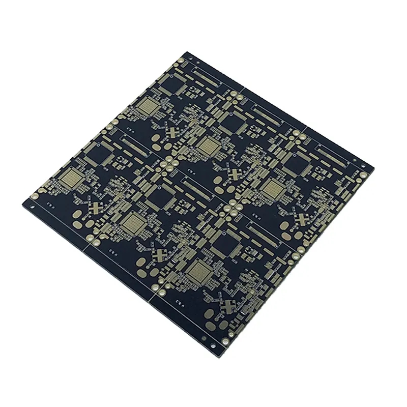
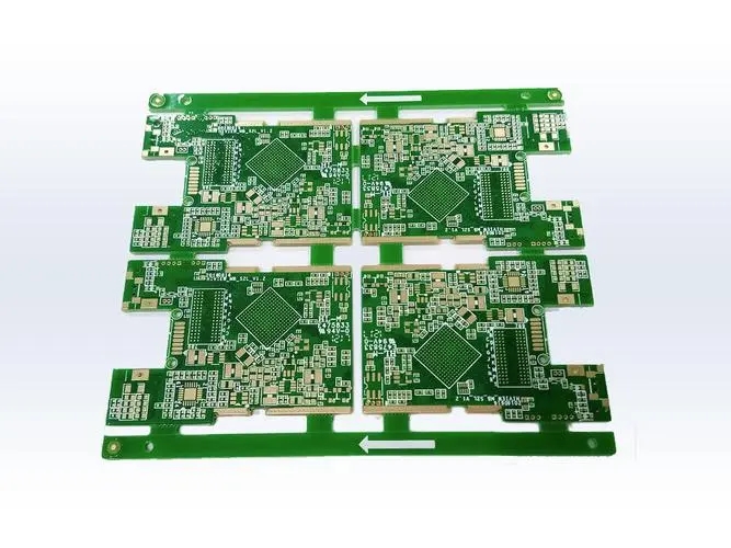
Since surface mount technology (SMT) began to gradually replace the jack mounting technology, the devices installed on the circuit board became smaller and smaller, and the functions contained in the unit area of the board became more and more powerful.
As far as passive surface mount devices are concerned, 0805 devices, which were widely used ten years ago, account for only about 10% of the total number of similar devices today; The consumption of 0603 device also began to decline four years ago, replaced by 0402 device. At present, the smaller 0201 device is becoming more and more popular. It took about ten years to change from 0805 to 0603. Undoubtedly, we are in an era of accelerated miniaturization. Then look at surface mount integrated circuits. From the Quadripartite Flat Package (QFP), which dominated ten years ago, to today's Flip Chip (FC) technology, a variety of packaging forms have emerged, such as thin small pin package (TSOP), spherical array package (BGA), and micro spherical array package( μ BGA), chip scale package (CSP), etc. Throughout the evolution of chip packaging technology, its main feature is that the surface area and height of devices are significantly reduced, while the pin density of devices is sharply increased. In terms of chips with the same logic function complexity, the area of flip chip devices is only one ninth of the area of the original quad flatpack devices, and the height is only about one fifth of the original.
Micro package components and high-density PCB bring new testing challenges
The shrinking size of surface mount devices and the subsequent high-density circuit installation have brought great challenges to testing. The traditional manual visual inspection is not suitable even for moderately complex circuit boards (such as single panel with 300 devices and 3500 nodes). It was once conducted that four experienced inspectors were asked to inspect the quality of solder joints of the same board four times. As a result, the first inspector found 44% of the defects, the second inspector and the first inspector had 28% consistency, the third inspector and the first two had 12% consistency, and the fourth inspector and the first three had only 6% consistency. This test exposed the subjectivity of manual visual inspection, which is neither reliable nor economical for highly complex surface mounted circuit boards. However, it is virtually impossible to visually inspect the surface mounted circuit boards using micro spherical array non package, chip scale package and flip chip.
Moreover, due to the reduction of pin spacing and the increase of pin density of surface mount devices, needle bed online testing is also facing the dilemma of "no foothold". According to the prediction of the North American Electronic Manufacturing Planning Organization, after 2003, it will not be possible to achieve satisfactory test coverage for surface mounted circuit boards with high-density packaging by using online testing. Based on the 100% test coverage in 1998, it is estimated that the test coverage will be less than 50% after 2003 and less than 10% after 2009. As for the problems of back current drive, test fixture cost and reliability that still exist in online testing technology, there is no need to consider more. Just because the test coverage is less than 10% in the future, this technology is doomed in the future.
Then, can we hand over the circuit board to the final functional test when human vision is not competent and the machine probe is nowhere to touch? Can we stand the test for several minutes, but only know whether the circuit board is broken or not, but do not know what happens in the "black box"?
The development of new testing experience technology brought about by optical testing technology will never stop because of the above difficulties. Testing and inspection equipment manufacturers have introduced products such as automatic optical inspection equipment and X-ray inspection equipment to meet the challenges.
In fact, these two devices have been widely used in the semiconductor chip manufacturing and packaging process before they were widely used in the circuit board manufacturing industry. However, they still need further innovation to truly cope with the test difficulties caused by the miniaturization of surface mount devices and high-density circuit boards.
At the same time, the major manufacturers of online testing and functional testing equipment in the industry have been unable to meet the future development trend. Their strategy is to quickly master relevant technologies and enter the market by acquiring relatively small manufacturers of automatic optical inspection equipment and X-ray inspection equipment.
Whether it is automatic optical inspection technology or automatic X-ray inspection technology, although they can help complete the work that manual visual inspection is not competent for, their reliability is not completely satisfactory. These technologies are highly dependent on computer image processing technology. If the information provided by the original optical image or X-ray image is insufficient, or the image processing algorithm is not effective, it may lead to false judgment. Fortunately, engineers have accumulated considerable experience in the application of optics and X-ray technology, so it is expected that in the next few years, the technology for generating optical images of high-resolution circuit boards and true three-dimensional X-ray images will make progress.
In addition, today's relatively cheap storage and computing technologies make it possible to process large capacity image information. What needs to be innovated in this field is the algorithm of image processing, and the combination of the most basic image enhancement and pattern recognition technology with expert system. These expert systems are based on the computer aided design and manufacturing data (CAD-CAM) of circuit boards, and combined with the experience data of production lines, they can conduct self-learning and self improve the algorithm of inspection and judgment. Another possible development direction in this field is to expand the range of spectrum. At present, the industry has begun to try to capture and analyze the infrared image of the circuit board when the board is powered on. By comparing the infrared image with the standard image, the points of "overheating" or "supercooling" are found to reflect the manufacturing defects of the board.
Online testing is at the end of its tether
For online testing technology, manufacturers and the industry are striving to seek such a goal: through as much information as possible about the electrical performance defects of circuit boards.
There are mainly three aspects of work being carried out around this goal:
The first is to strengthen the research, implementation and application of design for testability of circuit boards, including the use of boundary scan technology (digital devices: IEEE1149.1; hybrid devices: IEEE1149.4) and other built-in test technologies that have become industry standards.
The second is to make full use of circuit theory and circuit board CAD data to develop more advanced test algorithms. This algorithm makes it possible to calculate the electrical state of some other nodes by testing some nodes.
The third is to balance the resources of online testing and other testing equipment, and optimize the overall testing and inspection architecture.
However, despite these efforts, the importance and dominance of online testing have been shaken. On the contrary, the functional testing technology, which was relatively slow to develop due to the rise of online testing, will regain the momentum of development. PCB manufacturers, PCB designers and PCBA manufacturers will explain the development path of PCB testability technology.


Just upload Gerber files, BOM files and design files, and the KINGFORD team will provide a complete quotation within 24h.