
Professional PCB manufacturing and assembly
Building 6, Zone 3, Yuekang Road,Bao'an District, Shenzhen, China
+86-13410863085Mon.-Sat.08:00-20:00

PCB technology: CAM manufacturing methods and skills of HDI boards
PCB manufacturing, PCB design and PCBA processing manufacturers explain PCB technology decryption: CAM manufacturing methods and skills of HDI boards
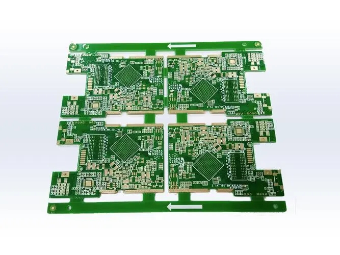
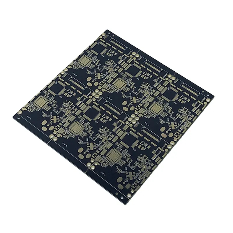
HDI board adapts to the requirements of the development of high integration IC and high-density interconnection assembly technology. It has pushed the PCB manufacturing technology to a new level and become one of the biggest hotspots of PCB manufacturing technology! In the CAM production of all kinds of PCBs, the personnel engaged in the CAM production agree that HDI mobile phone boards have complex shapes, high wiring density, and the CAM production is difficult to complete quickly and accurately! In the face of the requirements of customers for high quality and fast delivery, I have learned a little from my continuous practice and summary, and I would like to share this with my CAM colleagues.
1、 How to define SMD is the first difficulty in CAM production
In the process of PCB manufacturing, factors such as graphic transfer and etching will affect the final graphic. Therefore, we need to compensate the line and SMD respectively according to the customer's acceptance standard in CAM manufacturing. If we do not define SMD correctly, some SMD of the finished product may be smaller. Customers often design a 0.5mm CSP in the HDI mobile phone board, and its pad size is 0.3mm. In addition, some CSP pads are equipped with blind holes, and the pads corresponding to the blind holes are just 0.3mm, so that the CSP pads and the pads corresponding to the blind holes overlap or cross together. In this case, be careful to avoid mistakes. (Take genesis 2000 as an example)
Specific production steps:
1. Close the corresponding drilling layer of blind hole and buried hole.
2. Define SMD
3. Use the FeaturesFilterpopup and Referenceselectionpopup functions to find the pads of the include blind holes from the top layer and bottom layer, respectively moving to layer and b layer.
4. Use the Referenceselectionpopup function in layer t (the layer where the CSP pad is located) to select and delete 0.3mm pads touching the blind hole, and delete 0.3mm pads in the top layer CSP area. Then, according to the size, position and number of CSP pads designed by the customer, make a CSP and define it as SMD, then copy the CSP pads to the TOP layer, and add the pads corresponding to blind holes to the TOP layer. Layer b is made in a similar way.
5. Find out other SMDs with missing or multiple definitions according to the network file provided by the customer.
Compared with the conventional production method, it has clear purpose and fewer steps. This method can avoid misoperation and is fast and accurate!
2、 Removing non functional pads is also a special step in HDI mobile phone boards
Taking ordinary 8-layer HDI as an example, first remove the non functional pads corresponding to 2-7 layers of through-hole, and then remove the non functional pads corresponding to 2-7 layers of buried holes in 3-6 layers.
The steps are as follows:
1. Use the NFPRemovel function to remove the pad corresponding to the non-metallic holes on the top and bottom layers.
2. Close all drilling layers except through holes, select NO for RemoveuntrilLEDpads in the NFPRemovel function, and remove 2-7 layers of non functional pads
3. Close all drilling layers except 2-7 layers of embedded holes, select NO for Removeundrilledpads in NFPRemove function, and remove 3-6 layers of non functional pads
Using this method to remove non functional pads is clear and easy to understand, which is most suitable for people just engaged in CAM production
3、 About Laser Drilling
The blind hole of HDI mobile phone board is generally about 0.1mm micro hole. Our company uses CO2 laser. The organic material can strongly absorb infrared rays and ablate into holes through thermal effect. However, the absorption rate of copper to infrared rays is very small, and the melting point of copper is high, so CO2 laser cannot ablate copper foil, so we use the "conformalmask" process to etch the copper skin at the laser drilling hole with etching solution (CAM needs to make an exposure film). At the same time, in order to ensure that there is copper sheet in the secondary outer layer (bottom of laser drilling), the spacing between blind holes and buried holes should be at least 4mil. Therefore, we must use Analysis/Fabric/Board Drill Checks to find out the hole locations that do not meet the conditions.
4、 Plug hole and resistance welding
In HDI laminating configuration, the secondary outer layer is generally made of RCC material, with thin medium thickness and small glue content. According to the process experiment data, if the finished plate thickness is more than 0.8mm, the metallization groove is more than or equal to 0.8mmX2.0mm, and the metallization hole is more than or equal to 1.2mm, two sets of hole plug files must be made. That is to say, the plug hole is divided into two times. The inner layer is leveled with a resin, and the outer layer is directly plugged with solder mask ink before solder mask. In the process of resistance welding, vias often fall on or close to SMD. The customer requires that all vias be plugged, so when the solder mask is exposed, the vias with solder mask exposed or half of the holes exposed are easy to leak oil. CAM staff must deal with this. Generally, we prefer to remove the vias. If the vias cannot be removed, follow the steps below:
Add a light transmission point 3 MIL smaller than the one side of the finished hole on the solder mask layer at the through hole position of the covered window.
2. Add a light transmission point 3 MIL larger than one side of the finished hole on the solder mask layer at the through hole position of the solder mask opening touch. (In this case, the customer allows a little ink pad)
5、 Shape making
HDI mobile phone boards are generally delivered by assembly, with complex shape, and the customer attached a CAD drawing. If we use genesis 2000 to draw according to the drawings of customers, it will be very troublesome. We can directly click "Save As" in the CAD format file *. dwg to change the saving type to "AutoCADR14/LT98/LT97DXF (*. DXF)", and then read the * DXF files. The size and position of stamp hole, positioning hole and optical positioning point can be read as well as the shape, which is fast and accurate.
6、 Processing of milling outline frame
When processing the milling outline frame, unless the customer requires to expose the copper during CAM manufacturing, in order to prevent the plate edge from turning over the copper sheet, according to the manufacturing specifications, it is required to cut a little copper sheet from the frame to the inside of the plate, so it is inevitable that the situation shown in Figure 2A will occur! If both ends of A do not belong to the same network, and the width of copper sheet is less than 3mil (no figure may be made), it will cause an open circuit. There are no such problems in the analysis report of genesis 2000, so we must find another way. We can make one more network comparison, and in the second comparison, cut the copper sheet close to the frame into the plate by 3mil. If there is no open circuit in the comparison result, it indicates that both ends of A belong to the same network or the width is greater than 3mil (graphics can be made). If there is an open circuit, widen the copper sheet. PCB manufacturing, PCB design and PCBA processing manufacturers will explain PCB technology decryption: the CAM manufacturing methods and skills of HDI boards.


Just upload Gerber files, BOM files and design files, and the KINGFORD team will provide a complete quotation within 24h.