
Professional PCB manufacturing and assembly
Building 6, Zone 3, Yuekang Road,Bao'an District, Shenzhen, China
+86-13410863085Mon.-Sat.08:00-20:00

How to Improve the Integrity of PCB Signal in Embedded System
Circuit board manufacturing, circuit board design and PCBA processing manufacturers explain how to improve the integrity of embedded system PCB signals
With the continuous progress of electronic technology, more and more fields will be applied to embedded systems. Among these numerous applications, people no longer consider the function and performance, but the reliability and compatibility. Then, how to improve the signal integrity of embedded system PCB through wiring technology has become an "important topic".
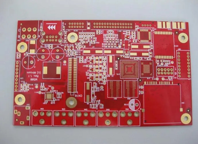
As we all know, PCB (printed circuit board) is the basic support of circuit components and devices in electronic products, and its design quality often directly affects the reliability and compatibility of embedded systems. In the past, in some low-speed circuit boards, the clock frequency is generally only about 10 MHz. The main challenge of circuit board or package design is how to route all signal lines on the double-layer board and how not to damage the package during assembly.
The electrical characteristics of the interconnects are not important because they do not affect system performance. In this sense, the interconnections in the low-speed signal circuit board are smooth and transparent. However, with the development of embedded systems, the circuits used are basically high-frequency circuits. As the clock frequency increases, the rising edge of the signal also becomes shorter. The capacitive reactance and inductive reactance of the printed circuit to the passing signal will be far greater than the resistance of the printed circuit itself, which seriously affects the integrity of the signal. For embedded systems, when the clock frequency exceeds 100 MHz or the rising edge is less than 1 ns, the signal integrity effect becomes important.
In PCB, signal line is the main carrier of signal transmission. The routing of signal line will directly determine the superiority of signal transmission, thus directly affecting the performance of the entire embedded system. Unreasonable wiring will seriously cause a variety of signal integrity problems, generate timing, noise and electromagnetic interference (EMI) on the circuit, and will seriously affect the embedded performance. In this paper, starting from the actual electrical characteristics of signal lines in high-speed digital circuits, the electrical characteristics model is established to find out the main reasons that affect signal integrity and the methods to solve the problems, and the problems that should be paid attention to and the methods and skills that should be followed in wiring are given.
Signal integrity
Signal integrity refers to the quality of the signal on the signal line, that is, the ability of the signal to respond with correct timing and voltage level in the circuit. Signal with good signal integrity refers to having the required voltage level value when needed. Poor signal integrity is not caused by a single factor, but by multiple factors in board level design. Signal integrity problems are reflected in many aspects, mainly including delay, reflection, crosstalk, overshoot, oscillation, earth bomb, etc.
Delay: The delay refers to that the signal is transmitted at a limited speed on the transmission line of the PCB board, and the signal is sent from the sending end to the receiving end, during which there is a transmission delay. Signal delay will affect embedded timing; The transmission delay mainly depends on the length of the wire and the dielectric constant of the medium around the wire. In high-speed digital systems, the length of signal transmission line is the most direct factor affecting the clock pulse phase difference. The clock pulse phase difference refers to that two clock signals generated at the same time do not arrive at the receiver synchronously. The phase difference of the clock pulse reduces the predictability of the arrival of the signal. If the phase difference of the clock pulse is too large, an error signal will be generated at the receiver.
Reflection: reflection is the echo of the signal on the signal line. When the signal delay time is far greater than the signal jump time, the signal line must be regarded as a transmission line. When the characteristic impedance of the transmission line does not match the load impedance, part of the signal power (voltage or current) is transmitted to the line and reaches the load, but part of it is reflected. If the load impedance is less than the original impedance, the reflection is negative; On the contrary, reflection is positive. Changes in wiring geometry, incorrect wire termination, transmission through connectors, and discontinuities in the power plane can cause such reflections.
Crosstalk: Crosstalk refers to the noise on signal lines caused by coupling between two signal lines, mutual inductance and mutual capacitance between signal lines. Capacitive coupling leads to coupling current, while inductive coupling leads to coupling voltage. Crosstalk noise originates from electromagnetic coupling between signal lines, between signal system and power distribution system, and between vias. Serial winding may cause false clock, intermittent data error, etc., and affect the transmission quality of adjacent signals. In reality, crosstalk cannot be completely eliminated, but it can be controlled within the range that the system can bear. PCB layer parameters, signal line spacing, electrical characteristics of the driver and receiver, and baseline termination mode have certain effects on crosstalk.
Overshoot and undershoot: Overshoot refers to the first peak or valley value exceeding the set voltage. For the rising edge, it refers to the highest voltage; For falling edge, it refers to the lowest voltage. Downrush refers to the next valley value or peak value exceeding the set voltage. Excessive overshoot can cause the protection diode to work, leading to its premature failure. Excessive undershoot can cause false clock or data errors (misoperation).
Oscillation and surround oscillation: The oscillation phenomenon is repeated overshoot and undershoot. The signal oscillation is caused by the inductance and capacitance transited on the line, which belongs to the under damping state, while the surrounding oscillation belongs to the over damping state. Like reflection, oscillation and surround oscillation are also caused by many factors. The oscillation can be reduced by proper termination, but it cannot be completely eliminated.
Ground level bounce noise and return current noise: when there is a large current surge in the circuit, it will cause ground level bounce noise. For example, when a large number of chip outputs are turned on at the same time, a large transient current will flow in the power plane of the chip and the board, and the inductance and resistance of the chip package and the power plane will cause power noise, which will produce voltage fluctuations and changes on the real ground plane, This noise will affect the action of other components. The increase of load capacitance, the decrease of load resistance, the increase of ground inductance, and the increase of the number of switching devices will lead to the increase of ground spring.
Analysis of electrical characteristics of transmission channel
In a multilayer PCB, most transmission lines are not only arranged on a single layer, but are staggered on multiple layers, and the layers are connected through vias. Therefore, in a multilayer PCB, a typical transmission channel mainly includes three parts: transmission line, routing corner and via. In the low frequency case, the printed wire and wiring via can be regarded as the common electrical connection connecting different device pins, which will not have too much impact on the signal quality. However, in the case of high frequency, the printed wire, corner and via can not only consider their connectivity, but also consider their electrical characteristics and parasitic parameters at high frequency.
Analysis of Electrical Characteristics of Transmission Lines in High Speed PCB
In the design of high-speed PCB, it is inevitable to use a large number of signal connecting lines with different lengths. Compared with the change time of the signal itself, the delay time of the signal passing through the connecting line cannot be ignored. The signal is transmitted on the connecting line at the speed of electromagnetic wave. At this time, the connecting line is a complex network with resistance, capacitance and inductance, which needs to be described by the distributed parameter system model, namely the transmission line model.
The transmission line is used to transmit signals from one end to the other. It consists of two wires with a certain length, one called the signal path and the other called the return path. In low-frequency circuits, the characteristics of transmission lines are shown as pure resistance electrical characteristics. In high-speed PCB, as the transmission signal frequency increases, the capacitive impedance between conductors decreases, and the inductive impedance on the conductor increases. The signal line will no longer only show pure resistance, that is, the signal will not only transmit on the conductor, but also transmit in the medium between conductors. If the signal frequency increases further, when j ω L>>R,1/(j ω C) <For uniform conductor, the average distribution of resistance R, parasitic inductance L and parasitic capacitance C of transmission line (i.e. L1=L2=...=Ln; C1=C2=...=Cn+1) without considering the change of external environment. PCB manufacturers, PCB designers and PCBA manufacturers will explain how to improve the integrity of PCB signals in embedded systems.


Just upload Gerber files, BOM files and design files, and the KINGFORD team will provide a complete quotation within 24h.