
Professional PCB manufacturing and assembly
Building 6, Zone 3, Yuekang Road,Bao'an District, Shenzhen, China
+86-13410863085Mon.-Sat.08:00-20:00

How much do you know about PCB reduction process?
PCB manufacturing, PCB design, PCBA processing manufacturer will explain PCB reduction process
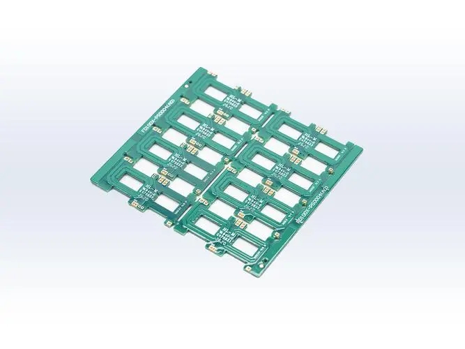
The reduction process is a method to selectively remove part of copper foil on the surface of copper clad laminate to obtain conductive patterns. The subtractive method is the main method of printed circuit manufacturing today. Its greatest advantage is that the process is mature, stable and reliable.
Printed circuits manufactured by subtractive process can be divided into the following two categories:
1. Non plating thr 'ough hole Board
Such printed boards are produced by screen printing and then etching, or by photochemical method. Non perforated plated printed boards are mainly single panel, and there are also a few double-sided boards, which are mainly used for TV and radio. The following is the single panel production process:
One side copper clad laminate blanking - photochemical method/screen printing image transfer - removing anti-corrosive printing material - cleaning and drying - hole processing - contour processing - cleaning and drying - printed solder resist coating - curing - printed symbol - curing - cleaning and drying - precoating flux - drying - finished product.
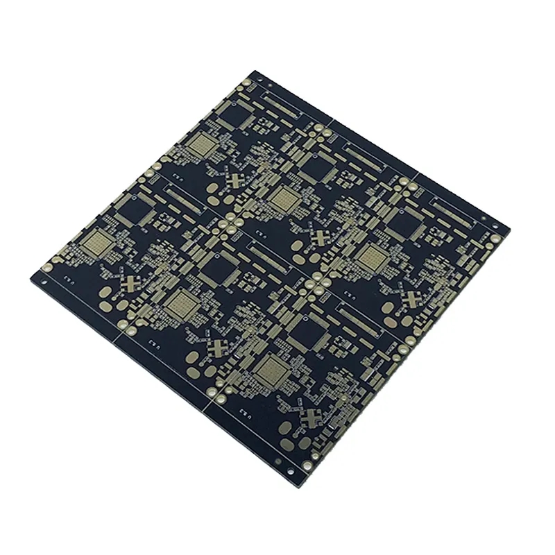
2. Plating through hole Board
On the copper clad laminate that has been drilled, electroless plating, electroplating and other methods are used to make the free L between two or more layers of conductive patterns from electrical insulation to electrical connection. Such printed boards are called perforated plated printed circuit boards. Perforated and plated printed boards are mainly used for computers, program-controlled exchanges, mobile phones, etc. According to different electroplating methods, it can be divided into graphic electroplating and full plate electroplating.
(1) Pattern electroplating (Pattern. n, P'I'N) On the double-sided copper clad laminate, a conductive pattern is formed by screen printing or photochemical method. The conductive pattern is plated with lead tin, tin cerium, tin nickel or gold and other corrosion-resistant metals, and then etched by removing the corrosion-resistant agent other than the circuit pattern. The pattern electroplating method is divided into pattern electroplating and etching process and solder mask OnBare Copper (SMOBC). The drop process of double-sided printed circuit board made of bare copper covered with solder mask is as follows:
Blanking of double-sided copper clad foil, punching of locating hole, numerical control drilling, inspection, deburring, chemical plating of thin copper, electroplating of thin copper, inspection, brushing, film pasting (or screen printing), exposure development (or curing), inspection, revision, graphic electroplating of copper, graphic electroplating of tin lead alloy, film removal (or printing material removal) One inspection revision, one etching, one lead and tin removal, one circuit breaking test, one cleaning, one solder resistance pattern, one plug nickel plating/gold, one plug adhesive tape, one hot air leveling, one cleaning, one screen printing mark symbol, one contour processing, one cleaning and drying, one inspection, one package, one finished product.
(2) Full plate electroplating (Panel, PNL) is applied to the double-sided copper clad laminate, copper is plated to the specified thickness, and then the image is transferred by screen printing or photochemical method to obtain the corrosion resistant normal phase circuit image. After corrosion, the corrosion inhibitor is removed to make the printed board.
The whole plate electroplating method can be subdivided into hole plugging method and masking method. The process flow of making double-sided printed boards with the masking method is as follows:
Blanking of double-sided copper clad foil, drilling, drilling, L, hole metallization, plating and thickening of the whole board, surface treatment, pasting, light masking, dry film, making normal phase conductor pattern, etching, film removal, plug electroplating, contour processing, inspection, printed solder resistance coating, solder coating, hot air leveling, printed marking symbols, and finished products.
The advantages of the above method are simple process and good uniformity of coating thickness. The disadvantage is that it wastes energy and it is difficult to make pcb without connecting plate. PCB manufacturing, PCB design and PCBA processing manufacturers will introduce PCB reduction process


Just upload Gerber files, BOM files and design files, and the KINGFORD team will provide a complete quotation within 24h.