
Professional PCB manufacturing and assembly
Building 6, Zone 3, Yuekang Road,Bao'an District, Shenzhen, China
+86-13410863085Mon.-Sat.08:00-20:00


Introduce the production process of circuit board
First, the PCB CAM data generated by CAD should be transferred to the PCB manufacturer. Circuit board manufacturers use CAM? 1 Data editor to check and edit film data, hole data, etc,
Add the reference mark and correction value required for making the circuit board or perform data synthesis. For example 1, check whether the spacing between the pad and the hole diameter is reasonable
Pads are usually tinned and the insert holes are hollow. From the pcb design, we can see that the pad is annular.
A few tenths of a millimeter is OK in the PCB design process, but in fact, manufacturers need to have a minimum width standard. The width design is too small to make. Above the usual design standards, the design standards need to be corrected according to the actual production standards of the circuit board manufacturers.
Circuit board production process
For example, the minimum width of the bonding pad: Some PCB manufacturers can achieve a minimum width of 0.2mm, and some manufacturers can achieve 0.25mm. It is impossible to ensure that the bonding pad can be formed if 0.2mm is required. For example 2, check the distance between the window opened on the solder mask and the pad.
Usually, a green film texture layer on a circuit board is a PCB solder mask layer. As the name implies, solder mask layers cannot be soldered normally.
The window of solder mask is usually designed to be larger than the diameter of PCB pad. This is to keep a certain distance between the window and the pad.
It is usually set to 0.2mm, so that even if there is some error on the plate, the solder mask will not be covered on the pad, resulting in poor welding. For example 3, check the minimum width of the routing and the minimum spacing of the routing. Generally, the minimum width and minimum spacing can be 0.2mm, respectively. When they are smaller, special PCB processes are required. Only the minimum standards that the manufacturer can achieve under normal circumstances are introduced here. For example 4, check the minimum distance between the edge of the circuit board or the non tinned through-hole (NPTH) and the routing.
·The minimum distance between the edge of the circuit board and the wiring is usually set as 1mm (0.5mm if necessary, not recommended) to prevent the wiring from being cut when the circuit board is divided.
Set to 3mm. When using machine welding components for circuit boards, due to the limitations of the actual machine, it can avoid damaging the wiring near the edges of the circuit boards.
·The contour line of pcb components (indicated by silk screen) should also be kept at least 1mm away from the edge of the circuit board (except for components whose positions are specified in the design).
The bonding pad of the component and the edge of the circuit board shall be at least 1mm, generally 3mm to 5mm. In addition to preventing splitting, it also reduces the fatigue brought to the pad and prevents the pad from falling off from the circuit board due to the relative stress.
·The minimum distance between the non tinned hole (NPTH) and the routing is determined by the use of the non tinned hole.
Generally, the distance between the through-hole of the component and the wiring is usually set to be more than 1mm (0.5mm if necessary, not recommended). For M3 screw holes, it is generally specified that wiring is prohibited and components are placed within 10mm in diameter. Prevent metal screws from touching the wiring, causing short circuit.
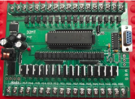
pcb
Note: The above minimum settings are the design standards of the circuit board, not the CAM settings. All the above checks can be performed by setting CAM? 3. After the inspection and correction work is completed, the data for various processing devices can be generated.
remarks:
1,CAM:Computer Aided Manufacturing
2. The pcb design standards mentioned here are based on the unwritten standards of the industry, which I have defined in the design. Readers need to refer to the standards of pcb manufacturers in pcb design to formulate their own design standards.
The old people said well, no rules, no square.
3. The set value of CAM is based on the standard limit that the manufacturer can generate circuit boards. Beyond this standard, it is impossible to produce a good circuit board.


Just upload Gerber files, BOM files and design files, and the KINGFORD team will provide a complete quotation within 24h.