
Professional PCB manufacturing and assembly
Building 6, Zone 3, Yuekang Road,Bao'an District, Shenzhen, China
+86-13410863085Mon.-Sat.08:00-20:00

An improved ladder process, which is characterized in that it comprises an upper layer substrate, at least one layer of middle layer substrate and a lower layer substrate. The PCB processis as follows: (1) Cutting: cutting the upper layer, middle layer substrate and lower layer substrate according to the required size; (2) Inner layer: the lower surface of the upper substrate, the upper surface of the lower substrate and the front and back surfaces of the middle substrate are formed into a circuit pattern by image transfer, and then the copper foil is removed by a target milling machine to form the required circuit pattern; Then the forming machine is used to fish the window of the middle layer substrate, and the window corresponding to the position and size is made on the middle layer substrate; (3) One time drilling: drill the aligned pin holes for the upper base plate, the middle base plate and the lower base plate; (4) Resin printing: the resin plug hole is selectively printed on the alignment pin hole drilled on the upper substrate, middle substrate and lower substrate; (5) Pressing: place films between the upper and middle layers of substrates and between the middle and lower layers of substrates and stack them in turn, use the positioning pins to align and stack them together, and send them to the vacuum press to harden and bond the films together through high temperature and high pressure to form multilayer circuit boards;
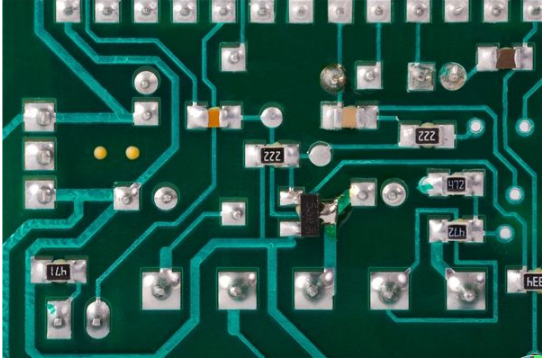
Circuit board production
Then, at the position where the step needs to be made, the forming machine is used to cut the upper substrate at a fixed depth to expose the upper surface line pattern of the lower substrate; (6) Secondary drilling: through the use of slot cutters of different specifications, drill slot holes of the required size on the multi-layer circuit board; (7) Electroplating: plating copper on the outer surface of multilayer circuit board and in the slot through chemical reaction, so that the slot can be conductive between layers; (8) Dry film: a layer of dry film is covered on the outer surface of the multilayer circuit board with copper, and a circuit image is formed on the outer surface of the multilayer circuit board with copper through image transfer; (9) Alkaline etching: remove useless copper foil by chemical reaction to obtain independent and complete outer circuit; (10) Soldering prevention: cover the outer surface of multilayer circuit board with a layer of ink by printing; (11) Printing: print corresponding symbols on the outer surface of multilayer circuit board by printing; (12) Forming: remove the useless frame of the whole multilayer circuit board, and then arrange it into the specified shape and specification after chemical cleaning.
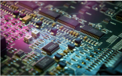
Problems encountered in pcb dry film circuit board production
With the rapid development of electronic industry, PCB wiring becomes more and more complex. Most PCBs use dry film for graphics transfer. The use of dry film is becoming more and more popular. However, in the process of after-sales service, many customers encounter many misunderstandings when using dry film. The summary is for reference.
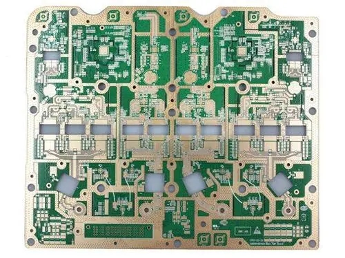
PCB proofing
Cracking of dry film covering hole
Many customers believe that the temperature and pressure of the film should be increased to enhance the adhesion after the occurrence of holes. In fact, this view is incorrect because the solvent of the resist volatilizes excessively after the temperature and pressure are too high. The dry film becomes brittle and thin, which is easy to crack during the development process. We always want to maintain the toughness of the dry film. Therefore, after the hole is broken, we can improve from the following points:
1. Reduce film temperature and pressure
2. Improve the drill bucket cloak
3. Increase exposure energy
4. Reduce development pressure
5. The parking time after shooting should not be too long, so as not to cause the semi fluid film at the corner to diffuse and become thinner under pressure
6. The dry film should not be too tight during shooting
Secondly, pcb dry film electroplating will occur when the circuit board manufacturer conducts electroplating
The reason for electroplating shows that the dry film and CCL are not firmly combined, so the electroplating solution is deep, and the "negative phase" electroplating layer is thickened. The electroplating of most PCB manufacturers is caused by the following points:
1. High or low exposure energy
Under the irradiation of ultraviolet light, the photoinitiator absorbing light energy decomposes into free radicals to induce luminous polymerization reaction, forming bulk molecules insoluble in dilute alkali solution. When the exposure is not sufficient, the polymerization is not complete. During the development process, the film expands and softens, resulting in unclear uniform lines on the film and poor adhesion between the film and copper; If overexposure will cause development difficulty, it will also occur in the electroplating process. Warp stripping occurs in the formation and electroplating is formed. Therefore, it is very important to control the exposure energy.
2. High or low film temperature
If the temperature of the pcb film is too low, the dry film and the copper-clad laminate may have poor adhesion due to insufficient softening and proper flow of the resist film; If the temperature is too high, it may cause the solvent and other volatilization in the resist. The rapid evaporation of the substance causes bubbles, the dry film becomes brittle, and warping and peeling are formed in the electroplating process, causing electroplating.
3. High or low membrane pressure
When the film pressure is too low, the film surface may be uneven or a gap may be formed between the dry film and PCB copper plate to meet the adhesion requirements; If the film pressure is too high, the solvent and volatile components of the resist layer will volatilize excessively, resulting in excessive evaporation. The dry film becomes brittle and will peel off after electroplating.


Just upload Gerber files, BOM files and design files, and the KINGFORD team will provide a complete quotation within 24h.