
Professional PCB manufacturing and assembly
Building 6, Zone 3, Yuekang Road,Bao'an District, Shenzhen, China
+86-13410863085Mon.-Sat.08:00-20:00

The wide application of SMT has promoted the miniaturization and multifunction of electronic products and provided conditions for mass production and low defect rate production. Surface mount technology is a new generation of electronic assembly technology developed from hybrid integrated circuit technology.
The main components of the SMT production line are: surface mounted components, circuit boards, assembly design, and PCB assembly process;
The main production equipment includes printing machine, dispensing machine, mounting machine, reflow soldering furnace and wave soldering machine. Auxiliary equipment includes testing equipment, repair equipment, cleaning equipment, drying equipment and material storage equipment.
1. According to the degree of automation, it can be divided into fully automatic production line and semi-automatic production line;
2. According to the size of the production line, it can be divided into large, medium and small production lines.
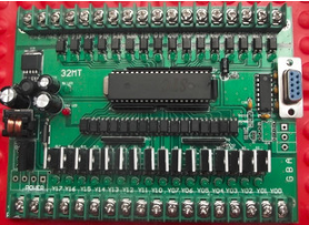
Pcb design
1、 Basic Process Composition of SMT
Screen printing (or dispensing)>pasting>(curing)>reflow welding>cleaning>detection>repair
2、 SMT production process flow
1. Surface mounting process
① Single side assembly: (all surface mounted components are on one side of PCB)
Incoming material detection - solder paste mixing - silk screen solder paste - patch - reflow soldering ② double-sided assembly; (Surface mount components are on both sides of PCB A and B respectively)
Incoming material detection - PCB A-side screen solder paste - patch - A-side reflow welding - flap - PCB B-side screen solder paste - patch - B-side reflow welding - (cleaning) - inspection - repair
2. Mixed charging process
① Single side mixed mounting process: (both plug-ins and surface mount components are on the A side of PCB)
Incoming material detection - solder paste mixing - PCB A-side silk printing solder paste - patch - A-side reflow welding - PCB A-side plug-in - wave soldering or dip welding (a small number of plug-ins can be manually welded) - (cleaning) - inspection - repair (paste first and then insert)
② Double side mixed packing process:
(Surface mount components are on the A side of PCB, and plug-ins are on the B side of PCB)
A. Incoming material detection - solder paste mixing - PCB A-side silk screen solder paste - patch - reflow welding - PCB B-side plug-in - wave soldering (a small number of plug-ins can be manually welded) - (cleaning) - inspection - repair
B. Incoming material detection - PCB side A screen printing solder paste - patch - manual solder inventory of PCB side A plug-in - PCB side B plug-in - reflow soldering - (cleaning) - inspection - repair
(Surface mount components are on the A and B sides of the PCB, and plug-ins are on either or both sides of the PCB)
First, reflow the surface mount components on both sides of A and B of the double-sided PCB according to the double-sided assembly method, and then manually weld the plug-ins on both sides.
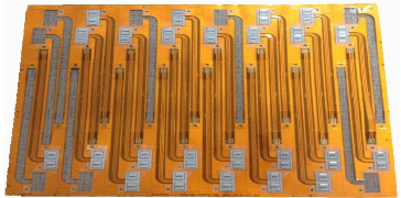
pcb
3、 Introduction to SMT process equipment
1. Formwork: (steel mesh)
First, determine whether to process the template according to the PCB design. If the patch components on the PCB are only resistors and capacitors, and the package is more than 1206, it is not necessary to make a template, but use a syringe or an automatic dispensing device to coat the solder paste; When the PCB contains chips packaged with SOT, SOP, PQFP, PLCC and BGA, as well as resistors and capacitors packaged below 0805, templates must be made. Generally, templates are divided into chemically etched copper templates (low price, applicable to small batch, test, and chip pin spacing of 0.635mm); Laser etching stainless steel template (high precision, high price, applicable to large batch, automatic production line, and chip pin spacing of 0.5mm). For R&D, small batch production or spacing of 0.5mm, it is recommended to use etched stainless steel templates; For the stainless steel formwork with mass production or spacing of 0.5mm, laser cutting is used. The overall dimension is 370 * 470 (unit: mm), and the effective area is 300 * 400 (unit: mm).
2. Silk screen printing: (high-precision semi-automatic solder paste printing machine)
Its function is to use a scraper to leak solder paste or paster onto the PCB pad, so as to prepare for the mounting of components. The equipment used is a manual silk screen printing stand (screen printing machine), a template and a scraper (metal or rubber), which is located at the front end of the SMT production line. It is recommended to use the medium size silk printing platform, and fix the template on the silk printing platform by using the precision semi-automatic silk printing machine method. Determine the position of PCB on the silk printing platform by using the up, down, left and right knobs on the manual silk printing platform, and fix this position; Then place the PCB to be coated between the screen printing platform and the template, place solder paste on the screen plate (at room temperature), keep the template parallel to the PCB, and evenly coat the solder paste on the PCB with a scraper. In the process of use, pay attention to the timely cleaning of the template with alcohol to prevent solder paste from blocking the leakage of the template.
3. Mounting: (Korean high-precision full-automatic multi-function mounting machine)
Its function is to accurately install surface mount components on the fixed position of PCB. The equipment used is a mounting machine (automatic, semi-automatic or manual), vacuum pen or tweezers, which is located behind the silk printing stand in the SMT production line. For laboratories or small batches, it is generally recommended to use double head anti-static vacuum suction pens. To solve the mounting and alignment problems of high-precision chips (chip pin spacing of 0.5mm), it is recommended to use Samsung full-automatic multi-function high-precision mounting machine (SM421 model can improve efficiency and mounting accuracy). The vacuum suction pen can directly pick up PCB resistance, capacitance and chip from the component rack. As the solder paste has certain viscosity, the resistance and capacitance can be directly placed on the required position; For the chip, a suction cup can be added to the vacuum pen holder, and the suction force can be adjusted through the knob. Keep in mind that no matter what components are placed, pay attention to the alignment position. If the position is misplaced, you must clean the PCB with alcohol, re screen, and re place the components.
4. Reflow soldering:
Its function is to melt the solder paste, so that the surface mounted components and PCB are firmly soldered together to achieve the electrical performance required by the design and precisely controlled in full accordance with the international standard curve, which can effectively prevent thermal damage and deformation of PCB and components. The equipment used is a reflow soldering furnace (full-automatic infrared hot air reflow soldering furnace), which is located behind the SMT mounter in the SMT production line.
5. Cleaning:
Its function is to remove the substances or welding residues, such as flux, that affect the electrical properties on the mounted PCB. If you use the cleaning free solder, you can generally do not need to clean it. Cleaning shall be carried out for products requiring low power consumption or high frequency characteristics. Generally, PCB products can be cleaned free. The equipment used is an ultrasonic cleaner or directly cleaned manually with alcohol, and the position can be unfixed.
6. Inspection:
Its function is to inspect the welding quality and assembly quality of the pasted PCB. The equipment used includes magnifying glass and microscope, which can be configured in the appropriate place of the production line according to the inspection requirements.
7. Rework:
Its function is to rework the PCB detected to be faulty, such as solder ball, solder bridge, open circuit and other defects. The tools used are intelligent soldering iron, repair workstation, etc. Configured anywhere in the production line.
4、 SMT auxiliary process: mainly used to solve the mixed process of wave soldering and reflow soldering.
1. Printing red glue: (red glue can be printed at the same time)
It is used to make red offset printing on the fixed position of PCB, mainly to fix components on PCB. It is generally used for surface mount components on both sides of PCB and wave soldering on one side. The equipment used is a printing machine. Solder paste and red glue printing can be completed by one machine, which is located at the front end of the SMT production line.
2. Curing: (Reflow soldering is better for curing and lead solder paste)
Its function is to heat solidify the patch adhesive, so that the surface mounted components and PCB are firmly bonded together. The equipment used is curing furnace (the reflow soldering furnace can also be used for curing adhesive and thermal aging test of components and PCB), which is located behind the SMT mounter in the SMT production line.


Just upload Gerber files, BOM files and design files, and the KINGFORD team will provide a complete quotation within 24h.