
Professional PCB manufacturing and assembly
Building 6, Zone 3, Yuekang Road,Bao'an District, Shenzhen, China
+86-13410863085Mon.-Sat.08:00-20:00


The conversion from soldering to lead-free type requires that the soldering temperature that the circuit board needs to withstand is extremely high, and the requirements for the thermal shock resistance of the surface are getting higher and higher. The requirements for the terminal surface treatment and the peel strength of the solder barrier layer (ink, covering film) are getting higher and higher, and the binding force with the base copper. We need a better effect of the pretreatment PCB process to guarantee this. Improve our process to improve product yield and gain profit growth points. High quality pre-treatment liquid medicine can undoubtedly help us at a low cost.
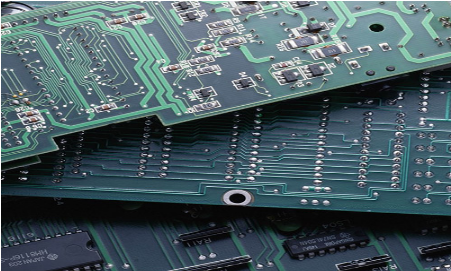
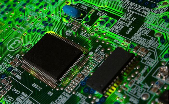
PCB
This paper mainly introduces the problems and countermeasures that are often encountered in the process of PCB rigid line PCB and FPB softness: First, side erosion and concavity occur when etching the circuit after dry film or wet film treatment in the circuit section, resulting in insufficient line width or uneven circuit. The reason lies in improper selection of dry and wet film materials, improper exposure parameters and poor performance of the exposure machine. The problems may be caused by unreasonable adjustment of nozzle and related parameters in developing and etching sections, improper concentration range of solution, improper transmission speed, etc. However, we often find that after checking the above parameters and the performance of related equipment, there is no abnormality. However, when making boards, there are still problems such as excessive corrosion and concave corrosion of circuit boards. What is the reason?
2、 In the process of PCB graphic electroplating, PCB and FPC terminal surface treatment, such as gold deposition, electrogold, electrolytic tin, and tin melting, we often find that the finished boards are infiltrated at the edge of the dry and wet film or the edge of the solder barrier layer, or most of the boards appear, or some places appear. No matter what kind of situation, it will lead to unnecessary scrap or defects, which will cause unnecessary trouble for the processing of the later section, or even the final scrap. It is heartbreaking! Through the cause analysis, people usually think that there are problems in the dry and wet film parameters and material properties; There is a problem with solder mask, such as printing ink for hard board and covering film for soft board, or there is a problem in printing, pressing, curing and other sections. Indeed, each of these places can cause this problem. Then we are also confused that there are no problems or problems have been solved in the above step section after inspection, but the phenomenon of plating still occurs. What are the reasons that haven't been found out?
3、 The PCB will be tin tested before shipment, and the customer will of course tin solder the components when using. It is possible that both stages may occur, or at a certain stage, tin dipping or soldering blistering will occur, and the substrate will be peeled off. Even when the adhesive tape is used to test the ink peel strength, the problem that the ink can be obviously peeled off or the peel strength of the covering film is insufficient or uneven will occur when the tensile test is used to test the peel strength of the soft board covering film. This kind of problem is absolutely unacceptable to customers, especially those who do precision SMT mounting. Once the solder mask peels off during welding, it will lead to the inability to accurately mount the original, causing customers to lose a large number of components and work delay. At the same time, the circuit board factory will face huge losses such as deduction, material replenishment, and even loss of customers. What aspects do we usually deal with when encountering such problems? We usually analyze whether it is a solder mask (ink, covering film) material; Is there a problem in the screen printing, laminating and curing stages; Is there a problem with the electroplating solution? wait... So we usually order engineers to find out the reasons and improve from these sections. We also wonder if it is the weather? Recently, it is relatively wet, and the boards absorb moisture? (Both the base material and the barrier are easy to absorb moisture) After a lot of hard work, we can get some results. The problem is temporarily solved on the surface. However, this kind of problem happens inadvertently, and what is the reason? Those sections that may have problems have obviously been checked and improved. What else did you not notice?
In view of the above widespread puzzles and problems in PCB and FPC industries. We have carried out a lot of tests and research, and finally found that an important reason for the problems such as poor circuit, infiltration, delamination, blistering, and insufficient peel strength is actually the pre-treatment part. Including wet and dry film pretreatment, welding resistance treatment, electroplating pretreatment, etc. Speaking of this, maybe many PCB industry people can't help laughing. Pretreatment is the simplest, including pickling, degreasing and micro etching. Many PCB technicians in the industry know which pre-treatment liquid, performance, parameters and even formula.


Just upload Gerber files, BOM files and design files, and the KINGFORD team will provide a complete quotation within 24h.