
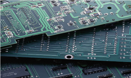
Professional PCB manufacturing and assembly
Building 6, Zone 3, Yuekang Road,Bao'an District, Shenzhen, China
+86-13410863085Mon.-Sat.08:00-20:00

The current electronic design of pcb proofing is mostly integrated system level design. the whole project includes both hardware design and software development. This technical feature presents new challenges to PCB engineers.
Pcb proofing
First, how to divide the system software and hardware functions reasonably in the early design stage to form an effective functional structure framework to avoid redundant cycle process;
Secondly, how to design high-performance and reliable PCB in a short time. Because the development of software largely depends on the realization of hardware, the design cycle will be shortened more effectively only if the whole machine design is passed once. This paper discusses the new characteristics and strategies of system board level design under the new technical background.
As we all know, the development of electronic technology is changing with each passing day, and the main reason for this change is the progress of chip technology. Semiconductor technology is becoming increasingly physical and has reached the level of deep submicron. Ultra large scale circuits have become the mainstream of chip development. However, this change in technology and scale has brought many new bottlenecks in electronic design throughout the entire electronic industry. Board level design has also been greatly impacted. One of the most obvious changes is the great variety of chip packages, such as BGA, TQFP, PLCC and other package types; Secondly, high-density pin packaging and miniaturization packaging have become a fashion to realize the miniaturization of the whole product, such as the extensive application of MCM technology. In addition, the increase of chip operating frequency makes it possible to increase the system operating frequency. These changes will inevitably bring many problems and challenges to board level design. First of all, due to the increasing physical limit of high-density pins and pin sizes, low throughput is caused; Secondly, the timing and signal integrity problems caused by the improvement of the system clock frequency; Third, engineers hope to use better tools to complete complex high-performance designs on the PC platform. From this, we can easily see that PCB design has the following three trends:
PCB design of high-speed digital circuits (i.e. high clock frequency and fast edge) has become the mainstream.
The miniaturization and high performance of products must face the problem of distribution effect caused by mixed signal design technology (digital, analog and RF mixed design) on the same board.
The improvement of design difficulty leads to that the traditional design process and design method, as well as the CAD tools on PC, are not competent for the current technical challenges. Therefore, the transfer of EDA software tool platform from UNIX to NT platform has become a recognized trend in the industry.
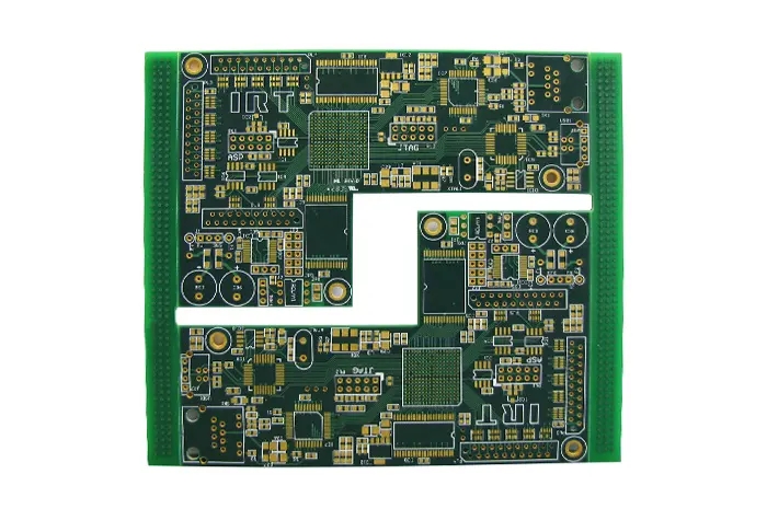
PCB board solution of high-speed digital system for pcb proofing
In general, when the signal interconnection delay is greater than 20% of the edge signal turnover threshold time, the signal wire on the board will show the transmission line effect, that is, the wire is no longer a simple wire performance that shows the lumped parameters, but a distributed parameter effect. This design is a high-speed design. In the design of high-speed digital systems, the designer must solve the problems of false switching and signal distortion caused by parasitic parameters - real-time sequence and signal integrity. At present, this is also a bottleneck problem that high-speed circuit designers must solve.
Traditional physical rule driven pcb proofing
We can find that in traditional high-speed PCB circuit design, electrical rule setting and physical rule setting are separated. This brings about the following defects:
At the early stage of PCB design, engineers had to spend a lot of energy on detailed front and back end (i.e., logical establishment physical implementation) analysis to plan a physical routing strategy to meet electrical requirements.
High speed effect is a complex subject, which can not be achieved by simply controlling the length of wiring and parallel lines.
The designer will inevitably face such a dilemma that the physical rules with false elements are not applicable in the actual wiring, and he has to modify the rules repeatedly to make them practical.
After the wiring is completed, the post validation tool can be used for analysis. However, if problems are found, engineers must return to the design and adjust the structure or rules. This is a cyclic redundant process. It will inevitably affect the time to market.
When there are only a few or dozens of key networks in the design, physical rule driven can well complete the design task; But when there are hundreds or even thousands of wire networks in the design, the physical rule driven method is not competent for the design task at all. The development of electronic technology calls for new methods and tools to solve the bottleneck problems faced by design. In order to solve the defects of physical rule driven high-speed design, the industry's knowledgeable people engaged in the research and development of high-speed digital circuit design EDA tools put forward the idea of real-time electrical rule driven physical layout and routing three years ago, and reformed the design idea of high-speed digital.
Pcb design
A new electric rule driven pcb proofing: interconnection synthesis
Interconnection synthesis is a typical term of real-time electrical rule driven method, that is, in the process of physical layout and routing, the interconnection synthesizer analyzes in real time according to the constraints of electrical rules, extracts the routing strategies that meet the requirements of the designer, and makes the design successful at one time. This method integrates electrical requirements and physical realization accurately through interconnection synthesis, and fundamentally eliminates the defects of physical rule driven method.
The integrated process of pcb proofing interconnection is as follows:
Input noise constraint and time order constraint rules in the tool;
Timing control layout to meet timing constraints;
Perform signal integrity pre optimization;
Board level integration to ensure that the key line network meets the electrical requirements;
Complete the wiring of ordinary wire network;
Comprehensive optimization of cabling.
The electrical rule driven method can effectively evaluate the quality before designing the layout and routing, detect the signal distortion, and determine the matching network topology and appropriate terminal matching structure and resistance value. After the layout and wiring is completed, post verification can be carried out, and the waveform can be intuitively detected with the software oscilloscope. The timing and distortion problems found at this time can be solved by the routing comprehensive optimization function.
Pcb proofing gold tool combination and design process
Now many EDA manufacturers can provide EDA tools for high-speed system PCB design to help users effectively improve design quality and shorten design cycle in this field. Among EDA system board level tools that apply electric rule driven method, the most representative is MentorGraphics ICX software package. It was the first to put forward the concept of interconnection integration, and it is also the most mature tool combination in the industry. This software package has the characteristics of plug and play, which is popular in the industry at present. It can be integrated in the classic EDA design process of PCB of many manufacturers.
Mixed signal design solution for pcb proofing
As the miniaturization of design has become fashionable, consumers need high-performance and low-cost goods. In order to adapt to market competition, manufacturers require R&D personnel to develop high-performance and low-cost products of different types and functional configurations in the shortest possible time to occupy the market. This brings designers many new design challenges. For example, using digital analog mixed technology, or even RF technology on the same substrate, to achieve the purpose of miniaturization of design and improvement of product functions. The mobile phone that is popular all over the world is a typical example. The industry also has corresponding solutions - design team, concurrent design, derivation and design reuse are the most typical strategies.
Traditional serial design of pcb proofing
That is, after the pcb engineer completes all the front-end circuit design, he will transfer it to the physical board level designer to complete the back-end implementation. The design cycle is the sum of circuit design and board level design time. After the miniaturization has become the mainstream design idea and the hybrid technology has been widely adopted, the serial design method has fallen behind. We must innovate in design methods and use powerful EDA tools to assist designers in design, so as to meet the requirements of timely listing. As we all know, it is impossible for each of us to become an expert in all fields, and it is impossible to complete all the work best and fastest in a short time. The concept of design team was put forward in this context and has been widely applied. At present, many companies adopt the method of design team to cooperate in product development. That is, according to the complexity of the design and different functional modules, the whole design is divided into different functional BLOCK blocks, and different designers and developers design logic circuits and PCB boards in parallel; Then, at the top level of the design, the final design results of each BLOCK block are called in as "devices" to form a whole board design. This method is called PCB design reuse. Through this method, we can see that it can greatly shorten the design cycle. The design time is only the sum of the design time of the BLOCK block that takes the most time and the time of the back-end interface connection processing.
Standardization of pcb proofing tools and integration of third-party tools
At present, many manufacturers are engaged in the development of pcb design automation (EDA) tools, such as Cadence, Synopsis, MentorGraphics as the main EDA tool suppliers; In addition, there are many other EDA manufacturers. EDA covers a wide range of fields, including network, communication, computer, aerospace, etc. The products involve system board design, system digital/IF analog/digital analog hybrid/RF simulation design, system IC/ASIC/FPGA design/simulation/verification, software and hardware co design, etc. It is difficult for any EDA supplier to provide the strongest design process to meet the different design needs of various users. From the perspective of market share, Cadence's strong products are IC board design and service, Synopsis's strong products are logic synthesis, MentorGraphics's strong products are PCB design and deep submicron IC design verification and testing. There is no doubt that modern electronic design increasingly relies on EDA tools and technologies. EDA manufacturers adopt the method of product standardization to meet the needs of users. Many designers adopt the strong products of multiple companies in their design process to form the best design process. EDA manufacturers have improved the compatibility of their strong products and the ability to integrate third-party products to meet the potential needs of users.
Derivation technology of pcb proofing
Pcb manufacturers, which focus on civil products, often need to develop products with different functions and grades to occupy the market in order to meet the needs of users at different levels. In the past, we often used different design processes to develop products with different functions, that is, to produce boards with different functions with different design data to realize products. The disadvantage is that the cost is increased and the design cycle is prolonged, and the artificial unreliable factors of products are increased. Now many manufacturers use derivative technology to solve the above problems, that is, to derive products with different function series from the same design process data, so as to reduce costs and improve quality. In order to meet the needs of users, many EDA manufacturers have added the Derived Rule Check (DRC) function to their products, such as MentorGraphics' BoardStation, Zuken Redac, etc. Taking BoardStation as an example, it provides complete functions, from the allocation of derived function modules in front-end circuit design to the physical layout rule check in the back-end, the generation of component list tables for different derived products, production and processing data Photo drawing data and processing assembly drawings, etc., thus completely ending this kind of PCB design puzzle.
Describe the production of pcb and fpc soft pcb
Nov 17,2022


Just upload Gerber files, BOM files and design files, and the KINGFORD team will provide a complete quotation within 24h.