
Professional PCB manufacturing and assembly
Building 6, Zone 3, Yuekang Road,Bao'an District, Shenzhen, China
+86-13410863085Mon.-Sat.08:00-20:00

Explanation of six types of PCB debugging technology modules
Circuit board manufacturing, circuit board design and PCBA processing manufacturers will explain the six types of modules of PCB debugging technology
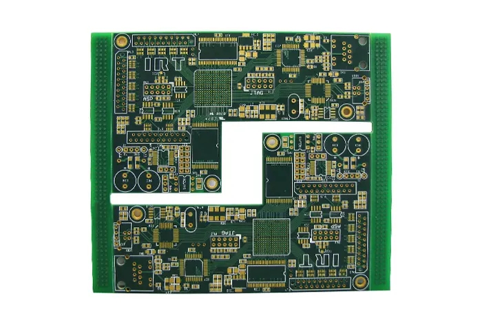
In PCB writing and design work, we often need to debug and test the circuit board. The debugging of six types of module circuit boards is one of them. In order to enable you to better understand the debugging technology of six types of module circuit boards, I will briefly introduce the six types of modules to you first. The important component of the six types of modules is the circuit board. Its design structure and manufacturing process basically determine the performance indicators of the product. The executive standard of the six types of modules is EIA/TIA 568B 2-1. The most important parameters are insertion loss, return loss, near end crosstalk, etc.
Category 6 Modules of PCB Debugging Technology
Insert Loss: due to the existence of transmission channel impedance, it will increase the attenuation of high frequency components of the signal as the signal frequency increases. The attenuation is not only related to the signal frequency, but also related to the transmission distance. With the increase of the length, the signal attenuation will also increase. Return Loss: Due to the change of impedance in the product, local vibration will occur, causing signal reflection. Part of the energy reflected to the sending end will form noise, causing signal distortion and reducing transmission performance. For example, a full duplex gigabit network will mistake the reflected signal for the received signal, causing fluctuations in the useful signal, causing confusion. The less reflected energy, the better the consistency of the impedance of the line used in the channel, and the more complete the transmission signal, the less noise on the channel. Calculation formula of return loss RL: return loss=transmitted signal ÷ reflected signal.
In the design, ensuring the consistency of the whole line impedance and cooperating with the six types of cables with 100 ohm impedance are effective means to solve the return loss parameter failure. For example, the uneven distance between layers of PCB lines, the change of copper conductor section of transmission lines, and the mismatch between conductors in modules and conductors of Category 6 cables will cause the change of return loss parameters. Near end crosstalk (NEXT): NEXT refers to the signal coupling between one pair of lines and another pair of lines in a pair of transmission lines, that is, when one pair of lines sends a signal, the signal received in another adjacent pair of lines. This kind of crosstalk signal is mainly due to that the adjacent pairs are coupled by capacitance or inductance. The main way to solve this parameter failure is to offset and weaken the interference signal by compensation, so that it cannot generate standing wave.
In the trial production stage of modules, with the guidance of theory and the basis of computer aided design, the expected results can be achieved quickly. In the design of six types of module PCB in China, a lot of trial production work is carried out mainly based on the line diagonal compensation theory, which can also achieve the desired results. The signal leakage caused by the module and the plug will cause mutual signal interference. To prevent signal interference, the conductor is twisted in the balanced link to achieve balanced transmission. The twisted structure will cause the phase change between signals and increase the signal attenuation on the line. This structure is called unshielded structure (UTP). In 4 pairs of balanced twisted pairs, the twist pitches of each pair of wires are different. Modular connectors are used at the end of the cable to form the connection between connectors and connectors. A balanced structure between conductors is formed in the interconnection area, which is a relatively long link of Category 6 systems. In a relatively long chain, the signal interference phenomenon occurred in the balanced line is called crosstalk. To solve the crosstalk problem is an important technology for manufacturing connectors for high-speed communication.
The contact loss between contact terminals will lead to attenuation, reflection loss and other phenomena. This loss will cause obstacles and faults when high-speed signal transmission occurs. Solving these problems is an important technology for manufacturing connectors for high-speed communication. In the connection line between the module and the plug, each pair of connection terminals in the plug is a balanced line, and the conductor in the balanced line will cause signal leakage and impedance loss. The relatively large factor impeding communication is signal leakage. This kind of problem can be solved by studying E field and H field or by studying the method of reverse attenuation, which is an important technology for manufacturing connectors for high-speed communication. The signal interference on the balance line of E field and H field, namely electromagnetic interference, can be described by the distribution of E field and H field.
The main parameter of the electronic communication line test is the correlation measurement under the sweep frequency. The higher the transmission speed, the faster the frequency. The solution of signal leakage is used to explain the problem of socket signal leakage. The basic method is to collect signals in the signal concentration area and send them back according to the simulation diagram of signal leakage caused by inductance and capacitance. In the design, the design of coupling capacitance is a key parameter, which is related to the length, distance between lines, width, compensation line layout, etc. of the coupling line. Considering that four pairs of lines are used to transmit signals simultaneously for six types of systems, it is inevitable to generate a comprehensive remote serial winding for them. Through analysis, computer simulation can be carried out to design a compensation line. The trial production process of six types of modules generally carried out by domestic peers is mainly to design a compensation circuit after the main circuit is determined, and carry out a large number of scheme design and sample production. After the compensation circuit and PCB interlayer structure are basically determined, the follow-up work is mainly to improve the performance through process improvement. PCB manufacturers, PCB designers and PCBA manufacturers will explain the six types of PCB debugging technology modules.


Just upload Gerber files, BOM files and design files, and the KINGFORD team will provide a complete quotation within 24h.