
Professional PCB manufacturing and assembly
Building 6, Zone 3, Yuekang Road,Bao'an District, Shenzhen, China
+86-13410863085Mon.-Sat.08:00-20:00

A good camera needs not only a good effect, but also an attractive appearance. Successful appearance design requires excellent design concept, but it also requires exquisite workmanship to embody this concept in specific objects.
Design 1. Appearance design According to the introduction of the pcb design team, the preliminary design of the camera is also very complicated.
The birth of a new camera was initially inspired by the designer. The designer first drew a sketch by hand to roughly reflect his ideas on paper and draw a simple general appearance.
After the ID group discussed and decided, use Rhino Rhino industrial modeling software to draw several 3D appearance effect pictures. After discussion and confirmation, send the rough appearance drawing file to the printing center for CNC 3D engraving and "hand printing", then review the solid model, and then constantly modify it according to the PCB model designer. This process is to confirm the final appearance of the camera to be achieved. After appearance proofing, the structure demonstration and design work will be carried out. Generally
"PRO-E" software, structural design.
When designing the base, many samples were printed. According to the market research, the designer found that the base of most cameras is a "clip", which can be used to clip laptops, but many LCD monitors with very personalized designs cannot be clipped, because the back plate is irregular. The designer specially designed a universal "hanging seat", which is a base designed according to the mechanical principle. It can be easily hung on the laptop and LCD display without clips, and can also be placed on the desktop or CRT display. This "hanging seat" takes a lot of effort. How to design materials and molds and how to produce molds have been discussed with the mold designer, and many samples have been made for testing. In the structural design stage, we need rich mold knowledge and a lot of communication with mold designers.
When the specific internal dimensions are determined, the designer can give the size of the PCB to the hardware engineer. At the same time, PCB design is also carried out synchronously from now on, and a lot of communication needs to be done between them. Sometimes, in order to fight for a little space, they fight with each other.
In order to check the fit between the structural dimensions and the PCB board, we also need to make a structural prototype. After testing, if there is a problem with the appearance or the internal structure does not conform to the PCB board, we can modify it. In fact, it is an iterative process to modify the appearance, until all the designs achieve the best coordination, and finally determine the mold, the PRO-E drawing will be formally handed over to the professional mold factory to manufacture the mold. From the appearance to the structure, this design takes the longest time, and there are many uncertain factors. It usually takes two or three months, and then it will be fast.
Process of appearance design: 1. Inspiration: hand drawn sketch
Confirm the general appearance 2. Practice: draw the general appearance with software pro-e or rhinoceros 3. Determine the initial color: use 3D
MAX renders 4. Pro-e is used to make the internal structure to achieve the appearance required 5. Make a manual version to confirm the appearance, check the structure and PCB coordination 6. Modify the structure diagram 7. Manufacture the mold (about 30 days)
pcb
2、 While determining the internal structure of the PCB design appearance, the hardware engineer can draw the schematic diagram according to the given internal structure size. The first step is to determine the plan. Since there are many options for the camera, the first step is to determine a good plan. Then you can start to draw the schematic diagram with POWER PCB software.
After the schematic diagram is drawn, convert it into a netlist, and then import the netlist into POWERPCB
And make it into a PCB file. Then start to draw the PCB board frame, and determine some fixed positions required by the mold, such as the positions of positioning holes, lights, and power sockets. Then layout and wire the PCB. The layout is mainly to ensure that the high-power components are separated from each other, and the filter capacitor is close to its corresponding IC pin; The main considerations for wiring are: the power supply and ground wire should be as thick as possible, and the wires that are easy to be disturbed should be protected.
Then it is to sort out the BOM, and check whether there are missing and extra components according to the schematic diagram. After checking, you can send the script. There is a certain time for the production of the prototype. After the completion of the production, it will be returned to the hardware engineer for component pasting and debugging. Debugging depends on the effect. If the effect is not satisfactory, continue to modify and debug to achieve the best effect repeatedly.
General design process: 1. Determine the scheme, such as Zhongxingwei 7131R+301L, or Magnum+Songhan 120 2. Draw the schematic diagram according to the scheme 3. Export the schematic diagram to a PCB file 4. Draw the PCB frame and the fixed position required by the mold 5. Layout and wire the PCB 6. Sort out the BOM 7. After checking, issue the manual 8. After returning the hand board, paste the components, and then debug 9. Start production after debugging
3、 The appearance design of mold manufacturing (the process takes about 30 days) has been determined, which is to turn the design in the concept into a mold in reality. This stage is carried out simultaneously with PCB design. Because it is a new mold, there are many problems to be solved from design to actual injection molding. Because if the product structure design is not reasonable, it is easy to cause various defects of the product: shrinkage, weld line, air hole, deformation, galling, top damage, flash. Therefore, mold manufacturing should comprehensively consider the processability of finished products and the performance of parts
Pay attention to the mold opening direction and parting surface, and try to eliminate the impact of parting line on the appearance to ensure the beauty and performance of the mold.
Final inspection is required after the mold is completed,
Confirm the shape difference between the product drawing and the real object (sample), confirm the surface roughness, strain and other problems, and also confirm the overall length, width, height and curvature.
Production Part I: Shell Production 1. Injection Molding
Once the mold is manufactured, it can be injected. Generally, at this stage, undesirable phenomena are easy to occur, such as insufficient filling, overflow, cracking, bubbles, etc., which need to be discussed and solved by the mold designer and the injection molding engineer. Therefore, every injection molding needs designers to spend a lot of energy to solve these problems and make the mold as perfect as possible.
2. Fuel injection process
The color of the appearance is determined. After a large amount of injection molding is carried out for the shell, the "material" is obtained, and then the process of oil injection is carried out. This process is absolutely a precise and rigorous process. A successful fuel injection requires such a 100000 level dust-free workshop. In order to get a good fuel injection effect, the key problem that must be solved first is how to remove the dust on the base material. The first step is to wipe the dust on the surface manually, perform the initial dedusting treatment, and then use the blower to blow the dust for secondary dedusting. The dedusting process is very important because it relates to the effect after spraying. The most important way of dedusting is "electrostatic dedusting". Fix the mold bottom materials after initial dedusting treatment on the support, about four in a group, and enter the "electrostatic precipitator cabinet" through the assembly line for thorough cleaning.
(Electrostatic dust removal spray gun)
After successfully dedusting, the mold will enter the "primer cabinet" through the assembly line. The primer needs to be sprayed several times. The base material installed on the bracket will rotate at a high speed during painting to keep the thickness of the paint uniform.
Shell painting
After the primer is sprayed, the finishing coat is sprayed, which is still the automatic operation of the assembly line, and finally the UV paint is sprayed. UV paint is the most important paint that can keep the top coat intact no matter if it is bumped or scratched with fingernails. After painting, the most important thing is drying, especially after spraying UV paint. If you let it dry, I'm afraid it will take a year! Therefore, ultraviolet radiation drying technology is required, and it only takes a short time to dry the paint.
(Because it is dried by ultraviolet ray, it cannot be taken close to the camera, and the strong light reflected inside can only be seen through the UV curing inspection port)
Oil spraying process
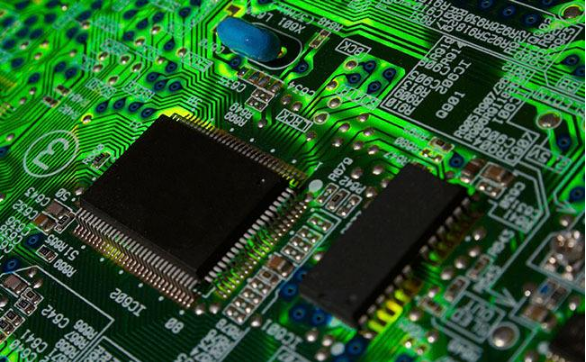
Pcb design
2、 The production of PCB board The production of PCB board and the production of shell are carried out at the same time. After mass production according to the designed PCB board documents and requirements, the placement is carried out according to the BOM and silk screen drawing, and the PCB components are welded according to the requirements. After the production is completed, the test shall be carried out to ensure that the products produced are qualified. This whole process is the complete PCB production.
First, paint solder paste for PCB board. Before brushing, PCB boards should be baked for more than 100 degrees to evaporate the water. Then the worker will check whether there are problems such as breakage on the PCB, and pick out the defective PCB. Leave qualified PCB boards with solder paste. Place the PCB under the special steel mesh plate, corresponding to the points where solder paste needs to be brushed. As soon as the above machine passes, the solder paste is evenly brushed on the PCB board. The steel mesh plate here is specially made for this camera. It should be noted that each steel mesh plate of different products is specially made to correspond to the place where solder paste needs to be painted.
(The solder paste is being applied, and the PCB board is at the corresponding position under the steel mesh board in the middle)
Roughly check whether the PCB board with solder paste is uniform, and then patch the PCB. The patch process is fully automatic. First, put the required materials into the corresponding loading tray, and use the computer to design the program. The placement machine accepts the automatic placement of various patch elements according to the program. Components such as SENSOR are "pasted" with a mounting machine.
(Automatic placement)
After pasting all components, check again for missing pasting. After that, the PCB board will be heated through the IR furnace, so that the solder paste and patch elements of the PCB board will be more bonded due to the heating after passing through the IR furnace. The requirements for the heat of the entire IR furnace are very strict, and it needs to be heated and reheated in several stages, which are also controlled by the computer program.
Since not all components can be automatically mounted, some must be welded, and some components cannot withstand the heat of the IR furnace. All PCB boards also need to be "post welded" to manually weld the remaining components, such as USB wire base, crystal oscillator, electric solution, resistance, etc.
After welding the components, check whether there is missing welding, false welding or faulty welding, and then repair welding.
In addition, there is a very important but easily overlooked link in the whole PCB production process: because the production process is inevitably sticky with dust, and in the bullet production, almost every production link will use a special cloth - fur to wipe the oil stains and dust off the COMS sensor surface, which is easy to lead to the imaging effect in the future because of the dust, and this process is even more important!
PCB production: 1. Brush solder paste 2. Patch 3. Pass through IR furnace 4. Post soldering 5. Repair soldering 6. Clean pcb
Assembly Part 1. After the assembly shell and PCB of camera parts are all produced, all parts need to be assembled. The so-called assembly is not a simple combination of them. The process is also quite delicate.
There are many processes in the assembly process at the same time. Here are some important processes.
First of all, introduce the lens installation: press the lens mouth into the lens cap with a hand beer machine. Before pressing in, check whether the lens mouth is damaged to ensure that the lens is intact. After pressing in, check whether there is a gap between the lens mouth and the cap. If there is a gap, it is an unqualified product and cannot be used.
After the lens is pressed in, the worker applies a layer of lubricating oil between the lens mouth and the cap. Because the aluminum alloy lens barrel and the plastic lens base are inevitably worn due to friction, adding a little lubricating oil can reduce this loss. This process is not done or omitted by many manufacturers.
Be careful to clean the lens to ensure the transparency and imaging clarity in the future. Then fix the produced PCB board and lens with screws, and install the lens adjusting ring.
At the same time, the shell is also being produced on another assembly line. First, check the shell and pick out all the defective parts such as scratches and wear. These are unqualified products and cannot be used. Then install the UBS cable into the shell. Then use screws to fix the upper part of the camera and the connecting rod of the base.
Clip the fixed PCB board and lens into the bottom of the housing, install the tail cover lamp, and then install the upper part of the housing. The upper and lower covers can be locked with screws. Finally, don't forget to wipe the dust off the lens.
The base needs to be pasted with QC and anti-counterfeit labels, and the bullet head needs to be fitted with foot pads. This work can be carried out simultaneously in another assembly line.
(Paste anti-counterfeiting label)
After all the accessories are assembled, the most important thing to do is to conduct a full QA inspection, such as checking the tightness of the lens focusing point, and further checking whether the assembled camera is scratched during the assembly process. If the camera is completely qualified, it is not only simple to assemble all the parts, but also the quality inspection before and after assembly. If the product quality is too high, you should not be careless in any details.
(Check the color difference against the color card)
(Check the tightness of the adjusting ring and the main body and the base)
2、 The packaging camera is assembled, and the rest is packaging. Put the instruction manual, CD, certificate of conformity, etc. into the color shell in order, and then put the inner bracket into the shell, so that the camera can be placed in the corresponding position. Before placing, it is still necessary to check whether the shell is damaged, and if there are scratches, it is unqualified. The barcode shall be pasted on the outer package in order. Then you can pack it!
A complete circuit product, the most important link is the design and production of pcb.


Just upload Gerber files, BOM files and design files, and the KINGFORD team will provide a complete quotation within 24h.