
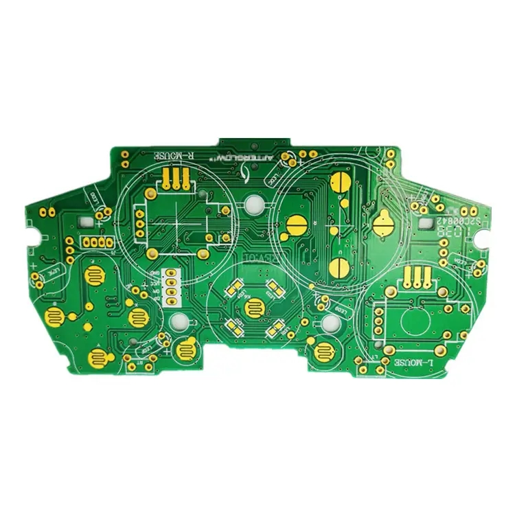
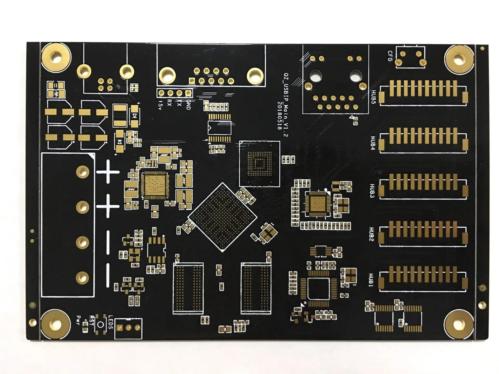
Professional PCB manufacturing and assembly
Building 6, Zone 3, Yuekang Road,Bao'an District, Shenzhen, China
+86-13410863085Mon.-Sat.08:00-20:00


How to check the spot welding quality during SMT chipprocessing
Nowadays, in order to meet the market demand, most electronic devices are developing towards precision machining and practical application. Even so, the electronic components of PCB are getting smaller and smaller, and the requirements for assembly accuracy are getting higher and higher. Electronic processing plants often need to use SMT chip processing technology to meet the needs of projects. The direct result of electric welding is that the quality and reputation of spot welding determine the quality of electronic equipment. How to ensure the quality of spot welding in SMT chip processing is a constant problem for electronic processing plants and SMT engineers. We also put forward many constructive suggestions and methods. How to check the quality of SMT chip processing spot welding?
1、 SMT spot welding inspection:
1. The surface must be fine, smooth and bright without defects; 2. The length width ratio of components shall be moderate, and there shall be an appropriate amount of welding materials and welding materials to completely cover the welding position of welding plates and leads; 3. Excellent wettability. The edges of welding points shall be relatively thin.
2、 Contents that must be checked for SMT production and processing appearance:
1. Whether to ignore this element; 2. Are the components correctly mounted? 3. Whether it will cause short circuit fault; 4. The components are not connected virtually and are not firm. Generally speaking, SMT chip processing shall be subject to visual inspection on the premise of fine spot welding of mechanical equipment and effective characteristics of mechanical equipment and electrical equipment to ensure the quality of electronic equipment. SMT chip processing and manufacturing industry is the foundation of electronic equipment manufacturing industry. What factors will damage the processing quality of SMT chip? A subtle key point and manufacturing stage will lead to quality problems of large and small products, unqualified inspection, delayed delivery, etc.
3、 The key conditions that endanger the SMT patch quality and cause the patch to lack parts are as follows:
The feeder of electronic equipment cannot feed in time; 2. The vacuum sucker of the module is blocked by the air supply, damaged by the vacuum sucker, and the proportion of the vacuum sucker to the width is incorrect; 3. Common faults and blockages in the real gas circuit of machines and equipment; 4. The circuit board is poorly picked up, causing deformation; 5. There is no solder paste or too little solder paste on the circuit board; 6. The quality of electronic equipment products is not consistent with the same thickness; 7. There are defects in the starting procedure flow of the mounter, or the main parameters of the thickness of the electronic equipment are not correctly selected when writing the program; 8. Knock it down accidentally due to human error.

How to Improve the Thermal Performance of PCB
1、 Thermal copper foil is added to PCB design, and large area power grounding copper foil is adopted. 1. The larger the contact area, the lower the junction temperature; 2. The larger the copper coverage area, the lower the junction temperature.
2、 Adding hot via to PCB design Adding hot via to PCB design can effectively reduce the junction temperature of the device and improve the temperature uniformity in the direction of the board thickness, which provides the possibility of using other heat dissipation methods on the back of the PCB. It is found through simulation that, compared with the device without heat dissipation via, the thermal power consumption of the device is 2.5W, the spacing is 1mm, and the center design is 6x6. The heat dissipation via can reduce the junction temperature by about 4.8 ° C, and the temperature difference between the top and bottom of the PCB is reduced from 21 ° C to 5 ° C. After changing the thermal through-hole array to 4X4, the junction temperature of the device is 2.2 ° C higher than that of 6x6, which deserves attention.
3、 PCB design IC back bare copper, reducing the thermal resistance between copper and air.
4、 PCB design layout optimization requires PCB design layout of high-power and thermal sensitive equipment.
1. The heat sensitive equipment shall be placed in the cold air area. 2. The temperature detector shall be placed at the hottest position. 3. On the same PCB device, the cooling air flow of the device with low heat generation or poor heat resistance (such as small signal transistor, small integrated circuit, electrolytic capacitor, etc.) should preferably be at the inlet, and the downstream cooling air flow of the device with high heat generation or good heat resistance (such as power transistor, large-scale integrated circuit, etc.) should be based on the size of heat generation and heat distribution. 4. In the horizontal direction, high-power equipment should be arranged as close to the edge of PCBA as possible to shorten the heat transfer path; In the vertical direction, high-power components should be arranged as close to the top of the printed circuit board as possible to reduce the impact of these components on the temperature of other components during operation. 5. The heat dissipation of the printed circuit board in the equipment mainly depends on the air flow, so it is necessary to study the air flow path in the design and reasonably configure the equipment or printed circuit board. The air flow tends to flow in places with low resistance, so please avoid leaAving large space in the area when configuring the equipment on the printed circuit board. The configuration of multiple printed circuit boards in the whole machine should also pay attention to the same problem. 6. Temperature sensitive equipment should be placed in the area with the lowest temperature (such as the bottom of the equipment), not directly above the heating equipment. Multiple equipment should be placed in a horizontal staggered layout. 7. The equipment with the highest power consumption and maximum heat is arranged near the best heat dissipation position. Do not place high-temperature equipment at the corners and edges of the printed circuit board unless there is a radiator nearby. When designing the power resistance, select the larger components as much as possible, and adjust the PCB design layout to make it have enough heat dissipation space.
Shenzhen Xingruixiang PCB design capacity Maximum signal design rate: 10Gbps CML differential signal; Maximum number of PCB design layers: 40; Minimum line width: 2.4mil; Minimum line spacing: 2.4mil; Minimum BGA PIN spacing: 0.4mm; Minimum mechanical hole diameter: 6mil; Minimum laser drilling diameter: 4mil; Maximum number of PINs:; 63000+Maximum number of elements: 3600; Maximum number of BGAs: 48+. PCB design service process 1. The customer provides schematic consulting PCB design; 2. Evaluate the quotation according to the schematic diagram and customer design requirements; 3. The customer confirms the quotation, signs the contract and prepays the project deposit; 4. Receive the advance payment and arrange the engineer to design; 5. After the design is completed, provide the document screenshot to the customer for confirmation; 6. The customer confirmed that it was OK, settled the balance and provided PCB design data.


Just upload Gerber files, BOM files and design files, and the KINGFORD team will provide a complete quotation within 24h.