
Professional PCB manufacturing and assembly
Building 6, Zone 3, Yuekang Road,Bao'an District, Shenzhen, China
+86-13410863085Mon.-Sat.08:00-20:00

PCB warping elements, lead-free welding and flip chip explanation
PCB board warping elements
In order to prevent the printed PCB from bending down excessively, it is important to properly support the PCB in the reflow furnace. PCB warpage is an essential factor that needs to be investigated in circuit assembly, and special description should be strictly carried out. Warpage of BGA or PCB caused by heat during reflow cycle will cause solder holes and leave a lot of residual stress on solder joint, forming early defects. The moire fringe projection impression system is used to simply depict this kind of warpage. This system can be operated online or offline, and is used to depict the features of pre disposed packages and PCB warpage. The off-line system can also simulate the reflow environment through the warping graphics based on the time/temperature coordinates set in the furnace for equipment and PCB.
Lead-free soldering
Lead free soldering is another new skill that many companies have begun to use. This skill started in the European Union and Japanese industry. At first, it was used to remove lead from soldering during PCB assembly. The date of completing this skill has been changing. At first, it was proposed to complete this skill in 2004, and later, it was proposed to complete this skill in 2006. However, many companies are now striving to have this skill in 2004, and some companies now supply lead-free products.
Now there are many lead-free solder alloys on the market, and the most common alloy composition in the United States and Europe is 95.6Sn/3.7Ag/0.7Cu. The disposal of these solder alloys is not much different from the disposal of Sn/Pb solder according to the specification. The printing and mounting processes are the same. The first difference is the reflow process, that is, it is necessary to select a higher liquid temperature for most lead-free solders. The peak demand temperature of Sn/Ag/Cu alloy is generally about 30 ℃ higher than that of Sn/Pb solder. In addition, it has been indicated that the reflow process window is much stricter than the standard Sn/Pb alloy.
As for small passive components, the number of vertical and bridging defects can also be reduced by reducing the same appearance, especially for 0402 and 0201 scale packages. In conclusion, the reliability of lead-free assembly shows that it is completely comparable to Sn/Pb solder, but the high temperature environment is outside, for example, the operating temperature in automobile use can exceed 150 ℃.
Flip chip
When the advanced skills at that time were integrated into the standardized SMT components, the skills encountered the greatest difficulty. Flip chip is widely used in BGA and CSP in the use of primary packaging components, although BGA and CSP have now selected the lead structure skill. In board level assembly, the use of flip chip can bring many advantages, including the reduction of component size, functional progress and cost reduction.
Unfortunately, it is necessary for manufacturers to increase their investment to select flip chip skills so as to upgrade the machine and add special equipment for flip chip technology. These devices include mounting systems and underfill drip coating systems that can meet the high precision requirements of flip chip. In addition, it also includes X-ray and acoustic image systems for weld detection after reflow welding and hole analysis after underfill.
Solder pad description, including shape, size and mask limitations, is critical for manufacturability and testability (DFM/T) and cost satisfaction.
Flip chip on PCB (FCOB) is mainly used in products that focus on miniaturization, such as Bluetooth module components or medical devices. A Bluetooth module printing board, in which flip chip technology is integrated with the same package as 0201 passive components. The same high-speed mounting and disposal of flip chip and 0201 equipment can also place solder balls around the package. This can be said to be a good example of standardizing the SMT assembly line and implementing advanced skills.
With high assembly density, small size and light weight of electronic products, the volume and weight of SMT components are only about 1/10 of those of traditional plug-in components. After SMT is generally used, the volume of electronic products is reduced by 40%~60%, and the weight is reduced by 60%~80%. High reliability and strong earthquake resistance. The solder joint defect rate is low. High frequency characteristics are good. Reduce electromagnetic and radio frequency interference.
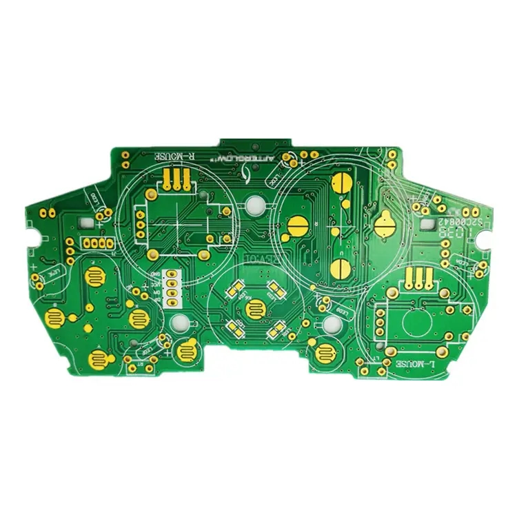
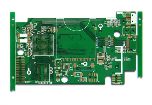
PCB manufacturing, PCB design and PCBA processing manufacturers will explain PCB warping elements, lead-free soldering and flip chip.


Just upload Gerber files, BOM files and design files, and the KINGFORD team will provide a complete quotation within 24h.